Intel Iris Pro 5200 Graphics Review: Core i7-4950HQ Tested
by Anand Lal Shimpi on June 1, 2013 10:01 AM ESTHaswell GPU Architecture & Iris Pro
In 2010, Intel’s Clarkdale and Arrandale CPUs dropped the GMA (Graphics Media Accelerator) label from its integrated graphics. From that point on, all Intel graphics would be known as Intel HD graphics. With certain versions of Haswell, Intel once again parts ways with its old brand and introduces a new one, this time the change is much more significant.
Intel attempted to simplify the naming confusion with this slide:
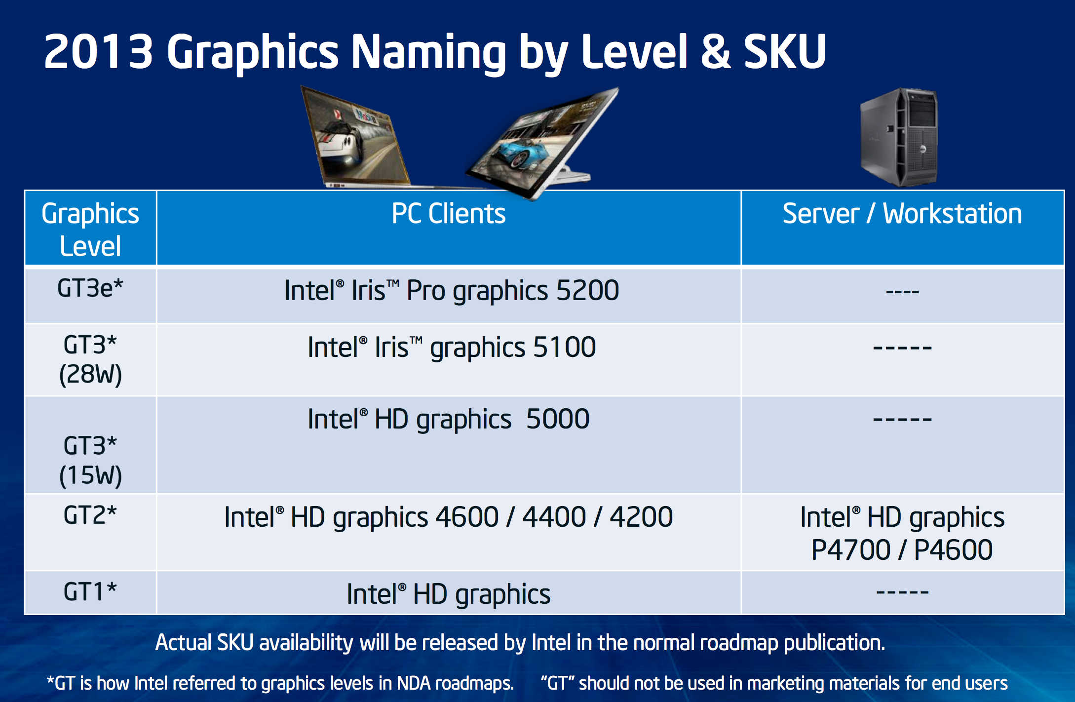
While Sandy and Ivy Bridge featured two different GPU implementations (GT1 and GT2), Haswell adds a third (GT3).
Basically it boils down to this. Haswell GT1 is just called Intel HD Graphics, Haswell GT2 is HD 4200/4400/4600. Haswell GT3 at or below 1.1GHz is called HD 5000. Haswell GT3 capable of hitting 1.3GHz is called Iris 5100, and finally Haswell GT3e (GT3 + embedded DRAM) is called Iris Pro 5200.
The fundamental GPU architecture hasn’t changed much between Ivy Bridge and Haswell. There are some enhancements, but for the most part what we’re looking at here is a dramatic increase in the amount of die area allocated for graphics.
All GPU vendors have some fundamental building block they scale up/down to hit various performance/power/price targets. AMD calls theirs a Compute Unit, NVIDIA’s is known as an SMX, and Intel’s is called a sub-slice.
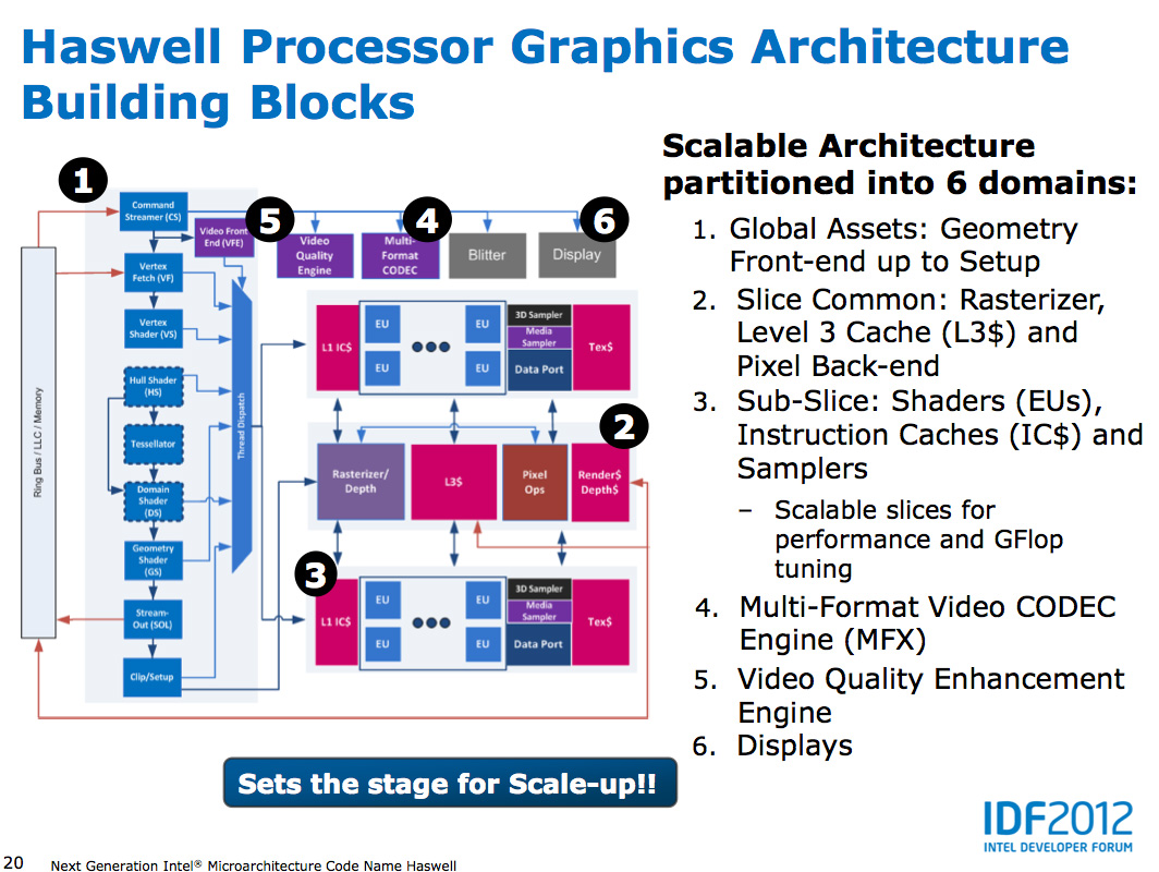
In Haswell, each graphics sub-slice features 10 EUs. Each EU is a dual-issue SIMD machine with two 4-wide vector ALUs:
| Low Level Architecture Comparison | ||||||||||||||||
| AMD GCN | Intel Gen7 Graphics | NVIDIA Kepler | ||||||||||||||
| Building Block | GCN Compute Unit | Sub-Slice | Kepler SMX | |||||||||||||
| Shader Building Block | 16-wide Vector SIMD | 2 x 4-wide Vector SIMD | 32-wide Vector SIMD | |||||||||||||
| Smallest Implementation | 4 SIMDs | 10 SIMDs | 6 SIMDs | |||||||||||||
| Smallest Implementation (ALUs) | 64 | 80 | 192 | |||||||||||||
There are limitations as to what can be co-issued down each EU’s pair of pipes. Intel addressed many of the co-issue limitations last generation with Ivy Bridge, but there are still some that remain.
Architecturally, this makes Intel’s Gen7 graphics core a bit odd compared to AMD’s GCN and NVIDIA’s Kepler, both of which feature much wider SIMD arrays without any co-issue requirements. The smallest sub-slice in Haswell however delivers a competitive number of ALUs to AMD and NVIDIA implementations.
Intel had a decent building block with Ivy Bridge, but it chose not to scale it up as far as it would go. With Haswell that changes. In its highest performing configuration, Haswell implements four sub-slices or 40 EUs. Doing the math reveals a very competent looking part on paper:
| Peak Theoretical GPU Performance | ||||||||||||||||
| Cores/EUs | Peak FP ops per Core/EU | Max GPU Frequency | Peak GFLOPs | |||||||||||||
| Intel Iris Pro 5100/5200 | 40 | 16 | 1300MHz | 832 GFLOPS | ||||||||||||
| Intel HD Graphics 5000 | 40 | 16 | 1100MHz | 704 GFLOPS | ||||||||||||
| NVIDIA GeForce GT 650M | 384 | 2 | 900MHz | 691.2 GFLOPS | ||||||||||||
| Intel HD Graphics 4600 | 20 | 16 | 1350MHz | 432 GFLOPS | ||||||||||||
| Intel HD Graphics 4000 | 16 | 16 | 1150MHz | 294.4 GFLOPS | ||||||||||||
| Intel HD Graphics 3000 | 12 | 12 | 1350MHz | 194.4 GFLOPS | ||||||||||||
| Intel HD Graphics 2000 | 6 | 12 | 1350MHz | 97.2 GFLOPS | ||||||||||||
| Apple A6X | 32 | 8 | 300MHz | 76.8 GFLOPS | ||||||||||||
In its highest end configuration, Iris has more raw compute power than a GeForce GT 650M - and even more than a GeForce GT 750M. Now we’re comparing across architectures here so this won’t necessarily translate into a performance advantage in games, but the takeaway is that with HD 5000, Iris 5100 and Iris Pro 5200 Intel is finally walking the walk of a GPU company.
Peak theoretical performance falls off steeply as soon as you start looking at the GT2 and GT1 implementations. With 1/4 - 1/2 of the execution resources as the GT3 graphics implementation, and no corresponding increase in frequency to offset the loss the slower parts are substantially less capable. The good news is that Haswell GT2 (HD 4600) is at least more capable than Ivy Bridge GT2 (HD 4000).
Taking a step back and looking at the rest of the theoretical numbers gives us a more well rounded look at Intel’s graphics architectures :
| Peak Theoretical GPU Performance | ||||||||||||||||
| Peak Pixel Fill Rate | Peak Texel Rate | Peak Polygon Rate | Peak GFLOPs | |||||||||||||
| Intel Iris Pro 5100/5200 | 10.4 GPixels/s | 20.8 GTexels/s | 650 MPolys/s | 832 GFLOPS | ||||||||||||
| Intel HD Graphics 5000 | 8.8 GPixels/s | 17.6 GTexels/s | 550 MPolys/s | 704 GFLOPS | ||||||||||||
| NVIDIA GeForce GT 650M | 14.4 GPixels/s | 28.8 GTexels/s | 900 MPolys/s | 691.2 GFLOPS | ||||||||||||
| Intel HD Graphics 4600 | 5.4 GPixels/s | 10.8 GTexels/s | 675 MPolys/s | 432 GFLOPS | ||||||||||||
| AMD Radeon HD 7660D (Desktop Trinity, A10-5800K) | 6.4 GPixels/s | 19.2 GTexels/s | 800 MPolys/s | 614 GFLOPS | ||||||||||||
| AMD Radeon HD 7660G (Mobile Trinity, A10-4600M) | 3.97 GPixels/s | 11.9 GTexels/s | 496 MPolys/s | 380 GFLOPS | ||||||||||||
Intel may have more raw compute, but NVIDIA invested more everywhere else in the pipeline. Triangle, texturing and pixel throughput capabilities are all higher on the 650M than on Iris Pro 5200. Compared to AMD's Trinity however, Intel has a big advantage.


177 Comments
View All Comments
tipoo - Saturday, June 1, 2013 - link
I really hope so, the Retina Macbook Pro 13" would get a whole lot more appealing with quad core and Iris Pro.DanNeely - Saturday, June 1, 2013 - link
Probably; easily if anand is right about Apple deciding it's good enough to drop the dGPU. Worst case would be Apple taking advantage of the adjustable TDP options to tune the CPU performance/tdp down a bit.Gaugamela - Saturday, June 1, 2013 - link
Really impressive!This focus of Intel on graphics will force Nvidia and AMD to push dedicated GPUs forward at a much faster pace at the risk of being destroyed by Intel iGPUs. This couldn't come at a better time with the advent of high resolution screens in notebooks and displays (that new 4K Asus monitor).
AMD will need to bring Kaveri with a monster of a iGPU otherwise Intel just nullified the only area where they had any type of advantage.
Blibbax - Saturday, June 1, 2013 - link
I question how much more can be had from APU graphics with the bandwidth restrictions of 64-bit DDR3.silverblue - Saturday, June 1, 2013 - link
Iris Pro is exceptionally good, however you have to ask how much faster the 7660D would be with the same memory bandwidth advantage. Additionally, Trinity is hardly going to be in the same sort of systems, and as the GPU is being held back by the CPU part anyway, it does take a little shine off Iris Pro's astounding performance. Even so, well done Intel, on both the hardware and software fronts.trulyuncouth1 - Saturday, June 1, 2013 - link
I think its kind of a moot point, Selling something this expensive will not affect AMD or even Nvidia that much. You can get an entire AMD APU based notebook for the cost of just this processor. I love the idea of this being pushed forward but unless Intel can bring it to a lower price point its kind of pointless.ilkhan - Saturday, June 1, 2013 - link
Im probably unique in that I want a quad haswell with the 20EU graphics and a GTX760m dGPU from a latitude (dock!) E6540. Wonder if thats going to happen. Probably not.Still, this looks damn good for Intel and will only improve over time.
lmcd - Sunday, June 2, 2013 - link
Howabout, rather, a 760 dGPU from a latitude dock? A bit more appealing :-)Zandros - Saturday, June 1, 2013 - link
Performance roughly in line with expectations, although the compute performance is a nice surprise. It seems to me like Crystalwell is going into exactly the wrong SKUs and the pricing is borderline atrocious, too.Anyway, since you bring up the awards and a "new system" for them, something I've been thinking a bit about is how there doesn't seem to be a page on the site where it is explained what each award is supposed to mean and collects all the products that have received them, which I think would be nice.
kallogan - Saturday, June 1, 2013 - link
Where is da power consumption ??????