Intel Iris Pro 5200 Graphics Review: Core i7-4950HQ Tested
by Anand Lal Shimpi on June 1, 2013 10:01 AM ESTHaswell GPU Architecture & Iris Pro
In 2010, Intel’s Clarkdale and Arrandale CPUs dropped the GMA (Graphics Media Accelerator) label from its integrated graphics. From that point on, all Intel graphics would be known as Intel HD graphics. With certain versions of Haswell, Intel once again parts ways with its old brand and introduces a new one, this time the change is much more significant.
Intel attempted to simplify the naming confusion with this slide:
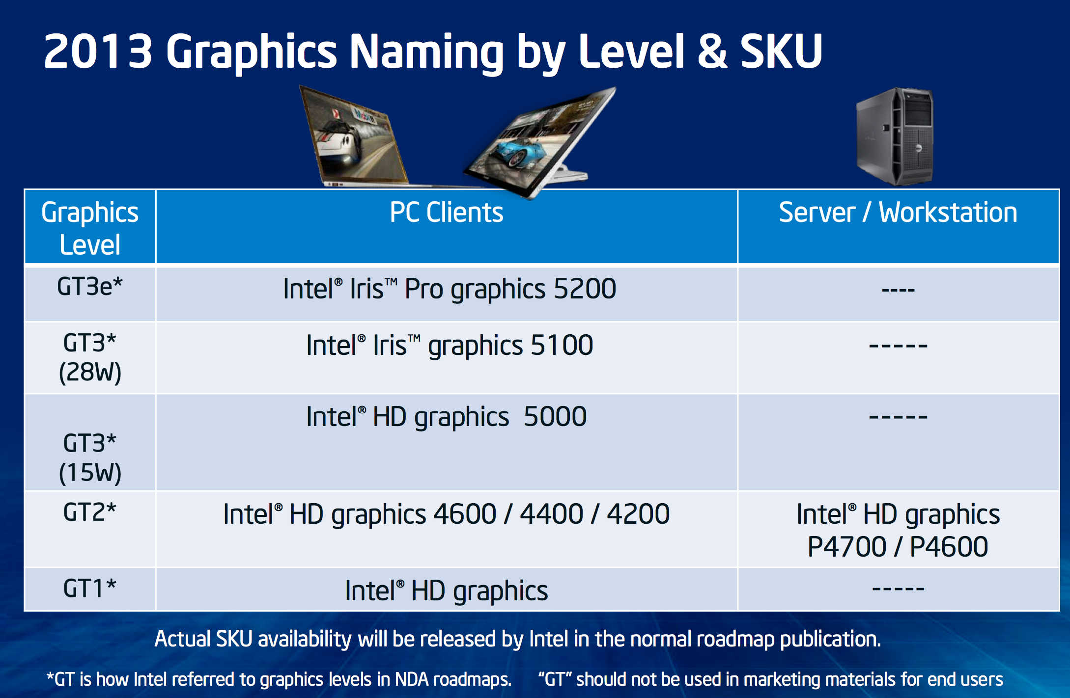
While Sandy and Ivy Bridge featured two different GPU implementations (GT1 and GT2), Haswell adds a third (GT3).
Basically it boils down to this. Haswell GT1 is just called Intel HD Graphics, Haswell GT2 is HD 4200/4400/4600. Haswell GT3 at or below 1.1GHz is called HD 5000. Haswell GT3 capable of hitting 1.3GHz is called Iris 5100, and finally Haswell GT3e (GT3 + embedded DRAM) is called Iris Pro 5200.
The fundamental GPU architecture hasn’t changed much between Ivy Bridge and Haswell. There are some enhancements, but for the most part what we’re looking at here is a dramatic increase in the amount of die area allocated for graphics.
All GPU vendors have some fundamental building block they scale up/down to hit various performance/power/price targets. AMD calls theirs a Compute Unit, NVIDIA’s is known as an SMX, and Intel’s is called a sub-slice.
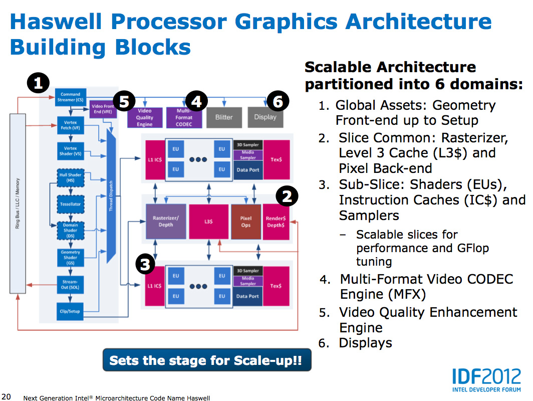
In Haswell, each graphics sub-slice features 10 EUs. Each EU is a dual-issue SIMD machine with two 4-wide vector ALUs:
| Low Level Architecture Comparison | ||||||||||||||||
| AMD GCN | Intel Gen7 Graphics | NVIDIA Kepler | ||||||||||||||
| Building Block | GCN Compute Unit | Sub-Slice | Kepler SMX | |||||||||||||
| Shader Building Block | 16-wide Vector SIMD | 2 x 4-wide Vector SIMD | 32-wide Vector SIMD | |||||||||||||
| Smallest Implementation | 4 SIMDs | 10 SIMDs | 6 SIMDs | |||||||||||||
| Smallest Implementation (ALUs) | 64 | 80 | 192 | |||||||||||||
There are limitations as to what can be co-issued down each EU’s pair of pipes. Intel addressed many of the co-issue limitations last generation with Ivy Bridge, but there are still some that remain.
Architecturally, this makes Intel’s Gen7 graphics core a bit odd compared to AMD’s GCN and NVIDIA’s Kepler, both of which feature much wider SIMD arrays without any co-issue requirements. The smallest sub-slice in Haswell however delivers a competitive number of ALUs to AMD and NVIDIA implementations.
Intel had a decent building block with Ivy Bridge, but it chose not to scale it up as far as it would go. With Haswell that changes. In its highest performing configuration, Haswell implements four sub-slices or 40 EUs. Doing the math reveals a very competent looking part on paper:
| Peak Theoretical GPU Performance | ||||||||||||||||
| Cores/EUs | Peak FP ops per Core/EU | Max GPU Frequency | Peak GFLOPs | |||||||||||||
| Intel Iris Pro 5100/5200 | 40 | 16 | 1300MHz | 832 GFLOPS | ||||||||||||
| Intel HD Graphics 5000 | 40 | 16 | 1100MHz | 704 GFLOPS | ||||||||||||
| NVIDIA GeForce GT 650M | 384 | 2 | 900MHz | 691.2 GFLOPS | ||||||||||||
| Intel HD Graphics 4600 | 20 | 16 | 1350MHz | 432 GFLOPS | ||||||||||||
| Intel HD Graphics 4000 | 16 | 16 | 1150MHz | 294.4 GFLOPS | ||||||||||||
| Intel HD Graphics 3000 | 12 | 12 | 1350MHz | 194.4 GFLOPS | ||||||||||||
| Intel HD Graphics 2000 | 6 | 12 | 1350MHz | 97.2 GFLOPS | ||||||||||||
| Apple A6X | 32 | 8 | 300MHz | 76.8 GFLOPS | ||||||||||||
In its highest end configuration, Iris has more raw compute power than a GeForce GT 650M - and even more than a GeForce GT 750M. Now we’re comparing across architectures here so this won’t necessarily translate into a performance advantage in games, but the takeaway is that with HD 5000, Iris 5100 and Iris Pro 5200 Intel is finally walking the walk of a GPU company.
Peak theoretical performance falls off steeply as soon as you start looking at the GT2 and GT1 implementations. With 1/4 - 1/2 of the execution resources as the GT3 graphics implementation, and no corresponding increase in frequency to offset the loss the slower parts are substantially less capable. The good news is that Haswell GT2 (HD 4600) is at least more capable than Ivy Bridge GT2 (HD 4000).
Taking a step back and looking at the rest of the theoretical numbers gives us a more well rounded look at Intel’s graphics architectures :
| Peak Theoretical GPU Performance | ||||||||||||||||
| Peak Pixel Fill Rate | Peak Texel Rate | Peak Polygon Rate | Peak GFLOPs | |||||||||||||
| Intel Iris Pro 5100/5200 | 10.4 GPixels/s | 20.8 GTexels/s | 650 MPolys/s | 832 GFLOPS | ||||||||||||
| Intel HD Graphics 5000 | 8.8 GPixels/s | 17.6 GTexels/s | 550 MPolys/s | 704 GFLOPS | ||||||||||||
| NVIDIA GeForce GT 650M | 14.4 GPixels/s | 28.8 GTexels/s | 900 MPolys/s | 691.2 GFLOPS | ||||||||||||
| Intel HD Graphics 4600 | 5.4 GPixels/s | 10.8 GTexels/s | 675 MPolys/s | 432 GFLOPS | ||||||||||||
| AMD Radeon HD 7660D (Desktop Trinity, A10-5800K) | 6.4 GPixels/s | 19.2 GTexels/s | 800 MPolys/s | 614 GFLOPS | ||||||||||||
| AMD Radeon HD 7660G (Mobile Trinity, A10-4600M) | 3.97 GPixels/s | 11.9 GTexels/s | 496 MPolys/s | 380 GFLOPS | ||||||||||||
Intel may have more raw compute, but NVIDIA invested more everywhere else in the pipeline. Triangle, texturing and pixel throughput capabilities are all higher on the 650M than on Iris Pro 5200. Compared to AMD's Trinity however, Intel has a big advantage.


177 Comments
View All Comments
Phrontis - Wednesday, June 5, 2013 - link
I can't wait for one on these on a mITX board such with 3 decent monitor outputs. Theres enough power for the sort of things I do if not for gaming.Phrontis
khanov - Friday, June 7, 2013 - link
Without a direct comparison between HD 5000/5100 and Iris Pro 5200 with Crystalwell,how can we conclude that Crystalwell has any effect in any of the game benchmarks? While it clearly is of benefit in some compute tasks, in the game benchmarks you only compare to HD 4600 with half as many EU's and to Nvidia and AMD with their different architectures.
We really need to see Iris Pro 5200 vs HD5100 to get an apples to apples comparison and be able to determine if Crystalwell is worth the extra money.
MODEL3 - Sunday, June 9, 2013 - link
Haswell ULT GT3 (Dual-Core+GT3) = 181mm2 and 40 EU Haswell GPU is 174mm^2.7mm^2 for everything else except GT3?
n13L5 - Tuesday, June 11, 2013 - link
" An Ultrabook SKU with Crystalwell would make a ton of sense, but given where Ultrabooks are headed (price-wise) I’m not sure Intel could get any takers."They sure seem to be going up in price, rather than down at the moment...
anandfan86 - Tuesday, June 18, 2013 - link
Intel has once again made their naming so confusing that even their own marketing weasels can't get it right. Notice that the Intel slide titled "4th Gen Intel Core Processors H-Processors Line" calls the graphics in the i7-4950HQ and i7-4850HQ "Intel HD Graphics 5200" instead of the correct name which is "Intel Iris Pro Graphics 5200". This slide calls the graphics in the i7-4750HQ "Intel Iris Pro Graphics 5200" which indicates that the slide was made after the creation of that name. It is little wonder that most media outlets are acting as if the biggest tech news of the month is the new pastel color scheme in iOS 7.Myoozak - Wednesday, June 26, 2013 - link
The peak theoretical GPU performance calculations shown are wrong for Intel's GFLOPS numbers. Correct numbers are half of what is shown. The reason is that Intel's execution units are made of of an integer vec4 processor and a floating-point vec4 processor. This article correctly states it has a 2xvec4 SIMD, but does not point out that half is integer and half is floating-point. For a GFLOPS computation, one should only include the floating-point operations, which means only half of that execution unit's silicon is getting used. The reported computation performance would only be correct if you had an algorithm with a perfect mix of integer & float math that could be co-issued. To compare apples to apples, you need to stick to GFLOPS numbers, and divide all the Intel numbers in the table by 2. For example, peak FP ops on the Intel HD4000 would be 8, not 16. Compared this way, Intel is not stomping all over AMD & nVidia for compute performance, but it does appear they are catching up.alexcyn - Tuesday, August 6, 2013 - link
I heard that Intel 22nm process equals TSMS 26nm, so the difference is not that much.alexcyn - Tuesday, August 6, 2013 - link
I heard that Intel 22nm process equals TSMC 26nm, so the difference is not that big.Doughboy(^_^) - Friday, August 9, 2013 - link
I think Intel could push their yield way up by offering 32MB and 64MB versions of Crystalwell for i3 and i5 processors. They could charge the same markup for the 128, but sell the 32/64 for cheaper. It would cost Intel less and probably let them take even further market share from low-end dGPUs.krr711 - Monday, February 10, 2014 - link
It is funny how a non-PC company changed the course of Intel forever for the good. I hope that Intel is wise enough to use this to spring-board the PC industry to a new, grand future. No more tick-tock nonsense arranged around sucking as many dollars out of the customer as possible, but give the world the processing power it craves and needs to solve the problems of tomorrow. Let this be your heritage and your profits will grow to unforeseen heights. Surprise us!