Intel Z87 Motherboard Review with Haswell: Gigabyte, MSI, ASRock and ASUS
by Ian Cutress on June 27, 2013 8:00 AM EST- Posted in
- Motherboards
- Intel
- MSI
- Gigabyte
- ASRock
- Asus
- Haswell
- Z87
- Shark Bay
- Lynx Point
While Anand deals with the detailed analysis of the Haswell CPU architecture and performance, a CPU is almost nothing without an accompanying chipset to provide connectivity and an interface with which to interact with the CPU. For our Z87 launch article all the major manufacturers sent us a motherboard to test, around the $200 mark, in order to showcase what we as users can expect from them in a reasonable price bracket. We also have managed to get hold of more of the nitty-gritty behind the Z87 platform, which has several features worth noting and talking about.
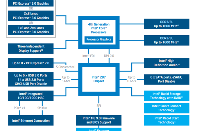
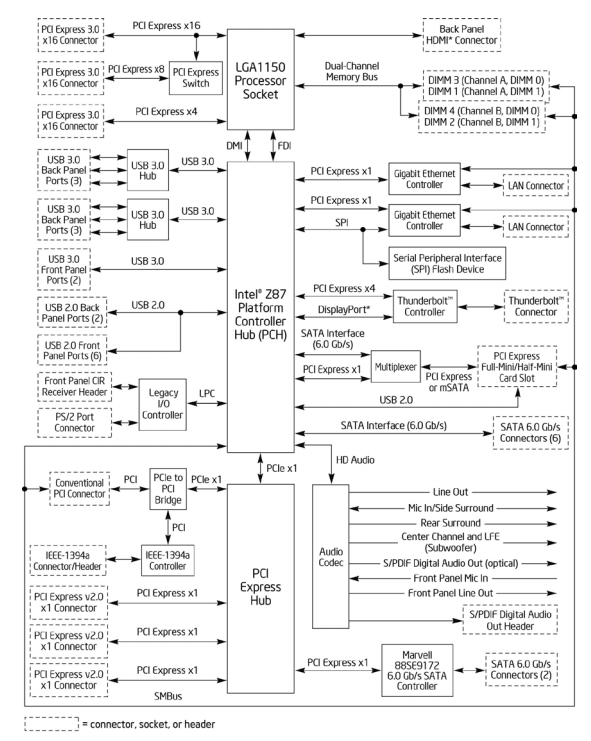
The Z87 Chipset
As consolidation occurs with parts of the system into the CPU, there could potentially be fewer and fewer opportunities for motherboard manufacturers to express their own individual take on each motherboard. Nonetheless, this has not stopped them coming up with gaming ranges, overclocking ranges, and using any number of controllers to provide additional functionality above and beyond the native Z87 chipset. Here is the chipset diagram for Z87 in a nutshell:
The first things to note are the lane allocations – we have a similar layout to Panther Point (Ivy Bridge) for 1x16, 2x8 or 1x8+2x4. The processor now takes control of the digital display outputs rather than the PCH, and can also deal with DDR3L memory. Natively the processor is set at 1333/1600 MHz, however from internal testing and from manufacturers almost every K-series SKU should handle DDR3-2400 at stock CPU speeds with ease.
On the chipset itself, we have a few new features – it is worth noting that it says ‘up to 8x PCIe 2.0, up to 6x USB 3.0 and up to 6x SATA 6 Gbps ports. This is a feature new to the consumer chipset range called Flex I/O.
Flex IO
Typically with a motherboard chipset we have a fixed number of SATA ports, a fixed number of PCIe lanes and a fixed number of USB ports. This is due to the fact that the PCH has them automatically wired in, and it is up to the motherboard manufacturer to connect the traces up within the Intel specified tolerances. Flex IO changes all this, into a mini-FPGA style arrangement, where several of the ports available can be configured to SATA 6 Gbps, PCIe or USB 3.0.
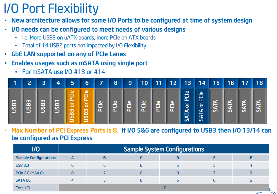
We get a total of 18 points in the architecture, of which four are USB 3.0, six are PCIe and four are SATA 6 Gbps. That leaves two pairs of two – the first pair can be assigned to USB 3.0 or PCIe, and the second pair can be assigned to SATA 6 Gbps or PCIe. The only limitation is that there can only be a maximum of eight PCIe 2.0 slots.
This allows motherboard manufacturers to position their SKUs very nicely – the PCIe 2.0 lanes can be split into extra USB 3.0 or SATA 6 Gbps controllers as well, meaning that on high storage platforms the manufacturer can go full out SATA 6 Gbps with controllers. There also remains the possibility that a motherboard manufacturer could assign all eight PCIe 2.0 lanes into a PCIe slot, giving that slot better bandwidth for multi-GPU scaling (at the expense of not being able to use those lanes for anything else such as PCIe x1).
The Intel Z87 Motherboard
Intel is still in the motherboard business for a couple of years, despite announcing their intention to leave the consumer motherboard market space. Like AMD, when it comes to media preview kits, they may call upon one of the motherboard manufacturers to supply the motherboard to send out of reviews. Until that day, we still get motherboards from Intel. Our Intel motherboard sample is in Anand’s hands right now for the CPU and IGP end of our motherboard coverage, but it looks a little something like this:
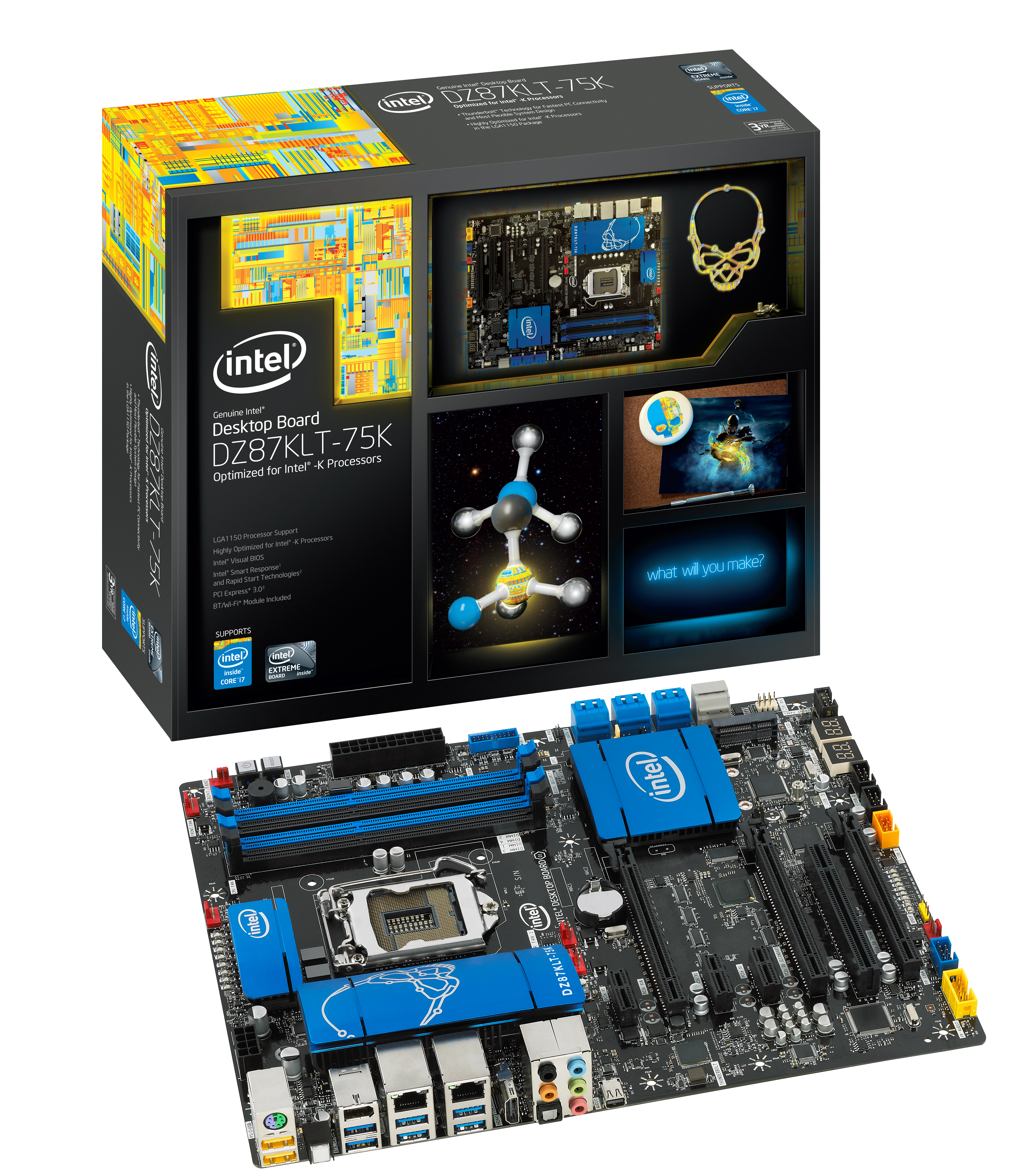
The reason why I bring up the Intel DZ87KLT-75K is that we have access directly to its chipset diagram:
Perhaps annoyingly, this is a little misleading – the chipset diagram suggests that we have a 20 PCIe lane processor when in actual fact the motherboard is an x8/x4/x4 layout. We can tell this because the PCH has all the 8x lanes being used – four for a Thunderbolt controller, two for Gigabit Ethernet, and one each for a USB 3.0 controller and a SATA 6 Gbps. This allows the motherboard to have a total of eight USB 3.0 and eight SATA 6 Gbps, which from what we have seen in our Z87 motherboard preview, is not too far-fetched.
What about H87 and others?
Intel is launching several chipset variations for Haswell processors, including H- for consumers as well as B- and Q- variants for business. The salient comparisons are as follows:
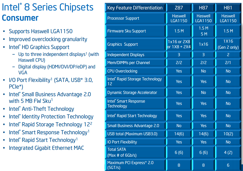
With H87 we lose CPU multiplier overclocking and multiple GPU configurations from the PEG lanes on the CPU. H81 takes it a little further, restricting displays, limiting the PCIe to Gen 2, and removing features such as RST, SRT and Flex IO.

Business chipsets follow on from the H87 chipset in terms of overclocking/GPU allocations, but typically come with business level features and support. For example, vPro needs a Q87 chipset, and B85 has fewer USB ports in total as well as not being iSIPP (Intel Stable Image Platform Program) eligible.


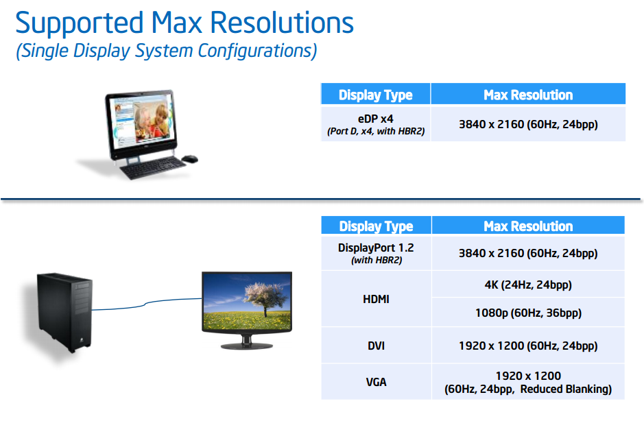
What about Display Configurations?
With “Shark Bay” (the platform combining a Haswell CPU and Lynx Point 8-series PCH), the ecosystem has moved the digital displays from the PCH to the CPU, leaving the VGA behind. This allows the system to integrate the S0ix power states a lot better than before, reducing idle power consumption and improving wake from sleep times (a main goal of Shark Bay). It also in some way allows Intel to have more control over the digital display allocations, especially dealing with WiDi. The platform now looks like:
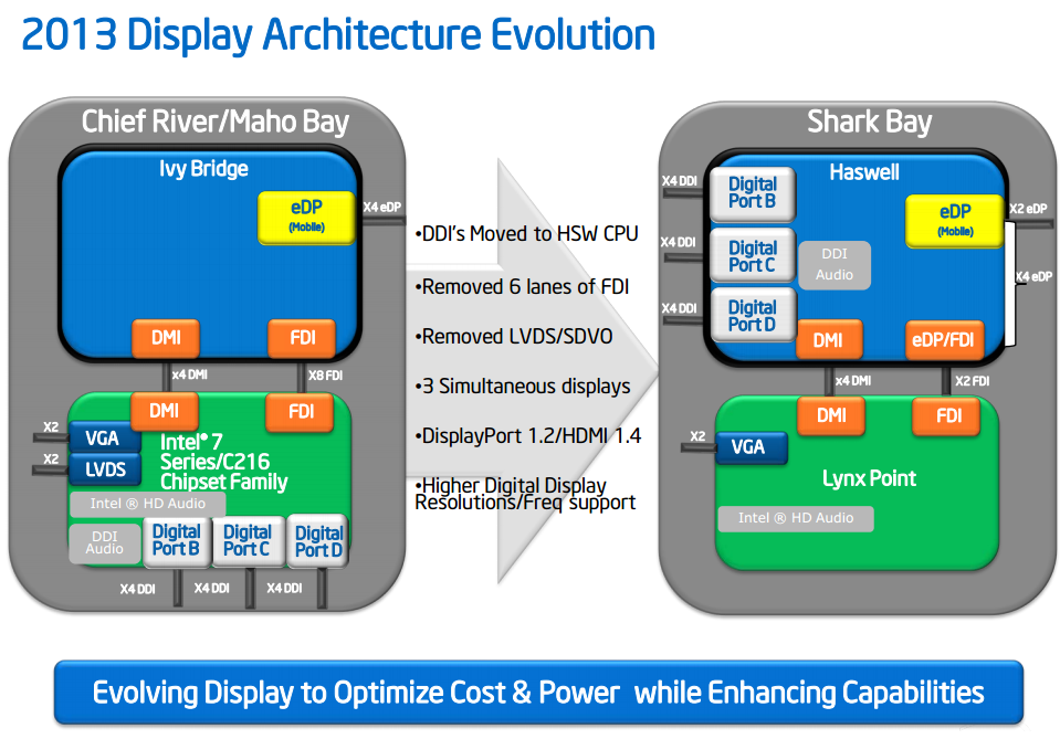
Arguably this may result in increased power consumption on the CPU, at the benefit of lower power consumption at the PCH (down 10%) which has to have a heatsink attached. But the digital ports, like with Panther Point, can be configured to a wide variety of digital outputs in a similar way to Flex IO.

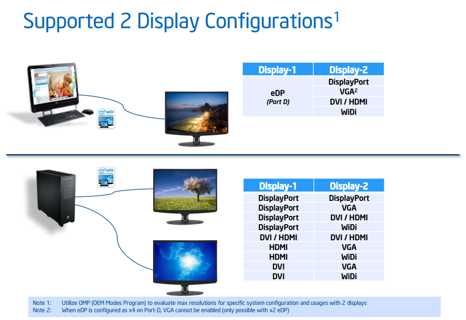
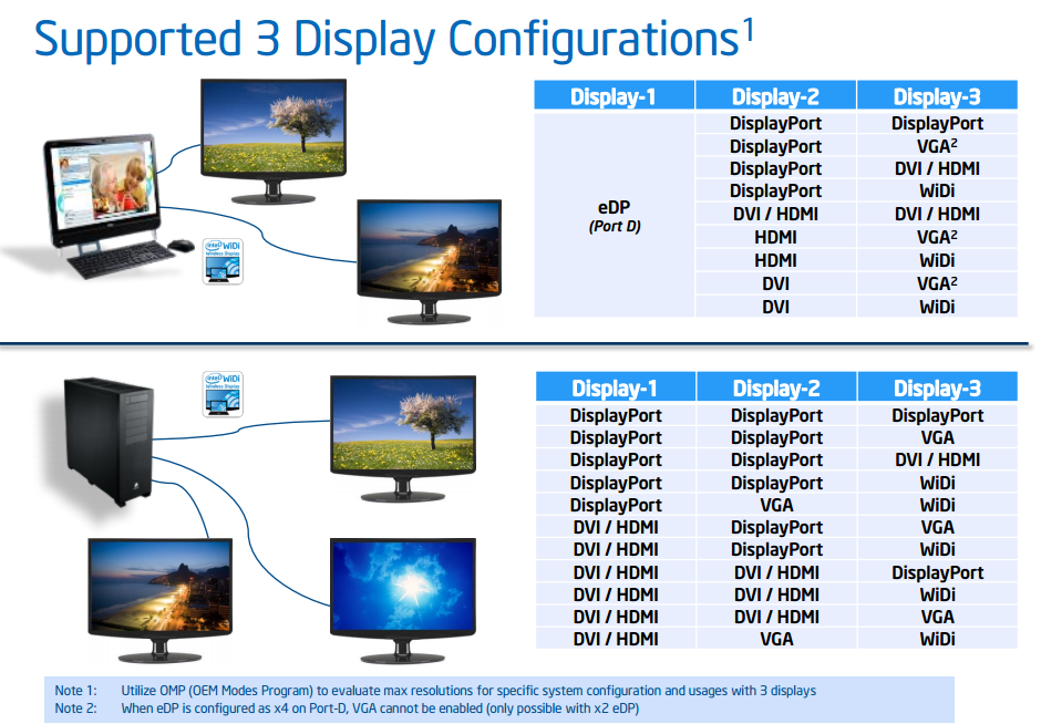
This is all from the processor itself of course – users with discrete GPUs will have different options from the GPU side of the equation.
What Did I hear about an Integrated Voltage Regulator?
As part of the consolidation, Intel is moving the voltage regulators onto the CPU to deal with various parts of the system onto the CPU itself. This means from a user perspective there should be less variation from the motherboard aspect in dealing with voltage inputs and quality, as only voltage needs to be pushed into the CPU for all the CPU features. Nonetheless it still means users will have to negotiate the internal voltages such as VCore in order to provide good overclocks. For extreme overclock users, it adds another element into potential CPU variation, meaning that searching for a good CPU may be a little bit more difficult.
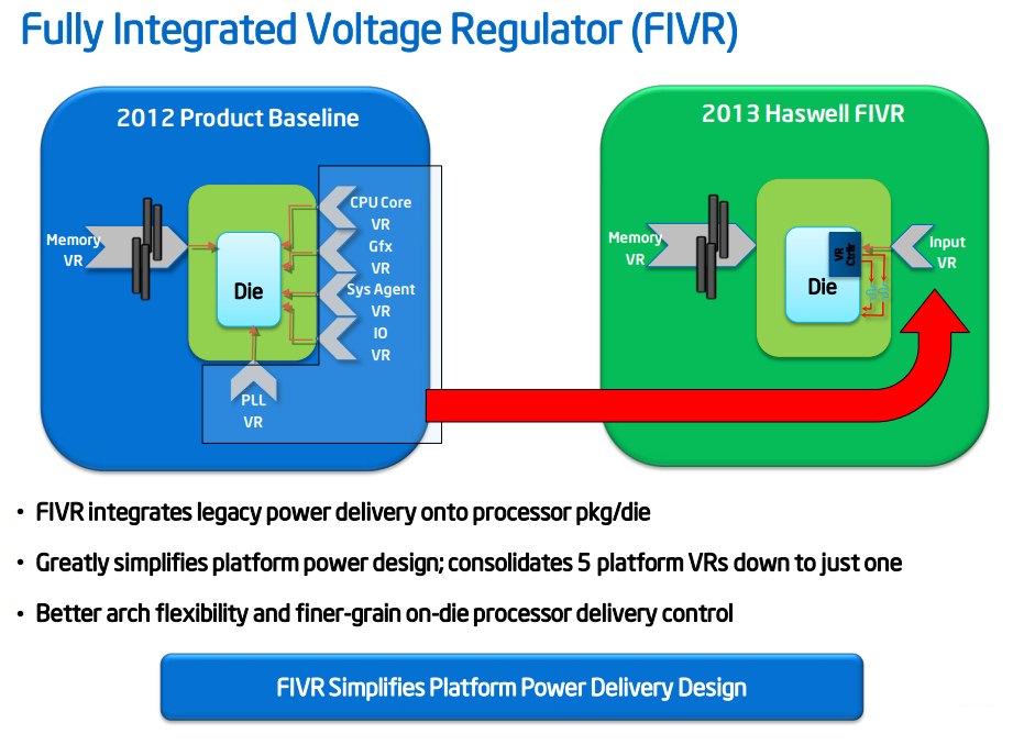
Anand has gone into greater detail in his Haswell coverage, but this also means that the integrated GPU can increase its speed and voltage without having to ‘wake’ the CPU part of the system up from a low power state unless needed.
Enough Already, Where Are The Motherboards?
For our first Haswell motherboard review, I asked the main manufacturers of such wondrous items to supply me with a motherboard around the $200 mark which would form the cornerstone of the high-end mainstream sales. Both our Sandy Bridge and Ivy Bridge initial coverage worked very well at this price point, and I begged the manufacturers to send samples to me as early as possible to we could pass more details on to our readers. While deadlines are tight, we managed to take on the following:
- Gigabyte Z87X-UD3H (MSRP $180, US Sale to $170)
- MSI Z87-GD65 Gaming (MSRP $190)
- ASRock Z87 Extreme6/AC (MSRP $220, US $20 Rebate for June)
- ASUS Z87-Pro (MSRP $210)
We also have another set of ASRock motherboards in to test, including the OC Formula and mini-ITX models, but unfortunately time to review these before launch day ran out, so they will be covered over the coverage.
First up to review is the motherboard that arrived in our offices first for testing – the Gigabyte Z87X-UD3H!


58 Comments
View All Comments
clyman - Tuesday, November 26, 2013 - link
In my personal experience and from ASUS tech support, the safest way to update bios is by first downloading it. This mobo has an excellent update program in bios that only looks at local drives, not online. I found it quite simple at each bios update.silenceisgolden - Thursday, June 27, 2013 - link
Great job Ian, really looking forward to the super high end motherboard review as well! I'm curious though, did you use the VGA port at all in any of these reviews, and also when was the last time you used a VGA port?IanCutress - Thursday, June 27, 2013 - link
My Korean 1440p panels are all via DVI-D. But the VGA comes in use when you have to use a DVI-I to VGA converter for DVI-I cables. Otherwise you need a DVI-D cable.JeBarr - Thursday, June 27, 2013 - link
Great review Ian. I very much appreciate your taking the time to explain the PCIe slot assignment and repeating the less-than-x8-no-good-for-SLI truth that needs to spread far and wide.What I took away from this review when analysing my own usage patterns and component choices is that each of the boards in this review would be better suited to the mATX form factor. There is no point in purchasing these mid-high end boards for multi-GPU, multi-display configs. There are only a handful of full size z87 boards that in my opinion earn their full-size status.
Shadowmaster625 - Thursday, June 27, 2013 - link
If it has fully integrated voltage regulators then why in blazes does it still need $20 worth of components buried beneath $3 heatsinks surrounding the cpu socket? Yeah, that's what I thought....DanNeely - Thursday, June 27, 2013 - link
What FIVR means to Intel isn't quite what you think it means. What's on package is the collection of VRs needed to provide power to all the separate sections of the CPU and to vary them as the chip clocks itself up and down. The motherboard itself still needs to do the heavy lifting to convert the 12V from the PSU to the voltage used by the DRAM and to a single input voltage the that CPU converts to the other levels it uses internally (IIRC this is the full load core voltage).I believe the reason why those regulators can be squeezed into the package while the ones still on the mobo are much larger is that the uncore/cache have relatively low power levels and the lower core voltages are only used at low CPU loads and thus don't need to push nearly as high of a peak current level.
WeaselITB - Thursday, June 27, 2013 - link
Wonderful review, Ian. Any chance of a Z87 vs Z77 vs ... comparison chart? It seems like functionalities of the processor are highly publicized, and the individual motherboard reviews chart the differences between chipset models within that family, but I don't recall seeing a comparison between chipset families. I know the chipset seems to be taking a smaller and smaller role these days, but it would still be helpful to exactly see the differences between generations.Thanks!
Kougar - Thursday, June 27, 2013 - link
It doesn't work with my 30" U3011 monitor either, yet another forum user with the same monitor didn't have any problem. Only difference was he used a Radeon and I use a GTX 480.
Creig - Thursday, June 27, 2013 - link
I only had time so far to skim this article, so I apologize if this question was already answered in the body. Is there any way to find out when each board starts shipping with the C2 stepping of the Z87 chipset? As some people are already aware, the C1 stepping has been shown to have issues with certain USB 3.0 controllers disconnecting when the computer awakes from sleep mode. The C2 stepping is apparently already shipping to manufacturers, but it would be handy to know a way to ensure that a person who orders a board in the near future receives the updated chipset.blackie333 - Friday, June 28, 2013 - link
I'm not sure that C2 stepping shipping already started, according to public available plan from May only samples have been sent to manufacturers. Mass production of C2 should start on 1st of July and manufacturers should start receiving them from the 30th of July. Boards based on C2 stepping should be available for end users from middle August.But you maybe have some more actual/insider information.