The Xbox One: Hardware Analysis & Comparison to PlayStation 4
by Anand Lal Shimpi on May 22, 2013 8:00 AM ESTMemory Subsystem
With the same underlying CPU and GPU architectures, porting games between the two should be much easier than ever before. Making the situation even better is the fact that both systems ship with 8GB of total system memory and Blu-ray disc support. Game developers can look forward to the same amount of storage per disc, and relatively similar amounts of storage in main memory. That’s the good news.
The bad news is the two wildly different approaches to memory subsystems. Sony’s approach with the PS4 SoC was to use a 256-bit wide GDDR5 memory interface running somewhere around a 5.5GHz datarate, delivering peak memory bandwidth of 176GB/s. That’s roughly the amount of memory bandwidth we’ve come to expect from a $300 GPU, and great news for the console.
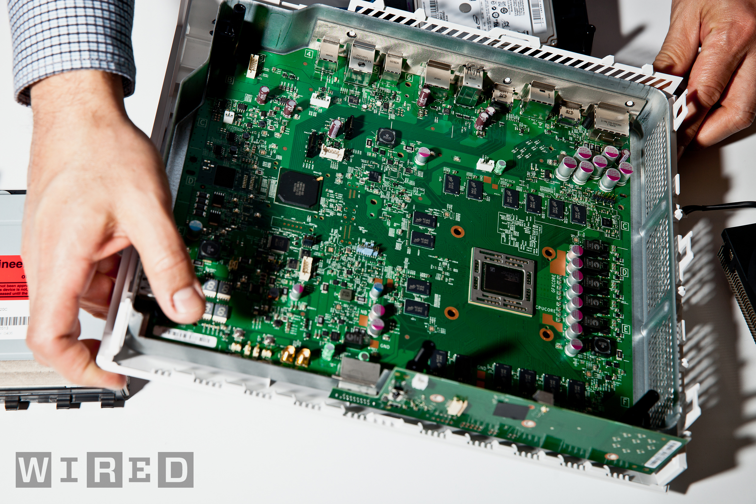 Xbox One Motherboard, courtesy Wired
Die size dictates memory interface width, so the 256-bit interface remains but Microsoft chose to go for DDR3 memory instead. A look at Wired’s excellent high-res teardown photo of the motherboard reveals Micron DDR3-2133 DRAM on board (16 x 16-bit DDR3 devices to be exact). A little math gives us 68.3GB/s of bandwidth to system memory.
To make up for the gap, Microsoft added embedded SRAM on die (not eDRAM, less area efficient but lower latency and doesn't need refreshing). All information points to 32MB of 6T-SRAM, or roughly 1.6 billion transistors for this memory. It’s not immediately clear whether or not this is a true cache or software managed memory. I’d hope for the former but it’s quite possible that it isn’t. At 32MB the ESRAM is more than enough for frame buffer storage, indicating that Microsoft expects developers to use it to offload requests from the system memory bus. Game console makers (Microsoft included) have often used large high speed memories to get around memory bandwidth limitations, so this is no different. Although 32MB doesn’t sound like much, if it is indeed used as a cache (with the frame buffer kept in main memory) it’s actually enough to have a substantial hit rate in current workloads (although there’s not much room for growth).
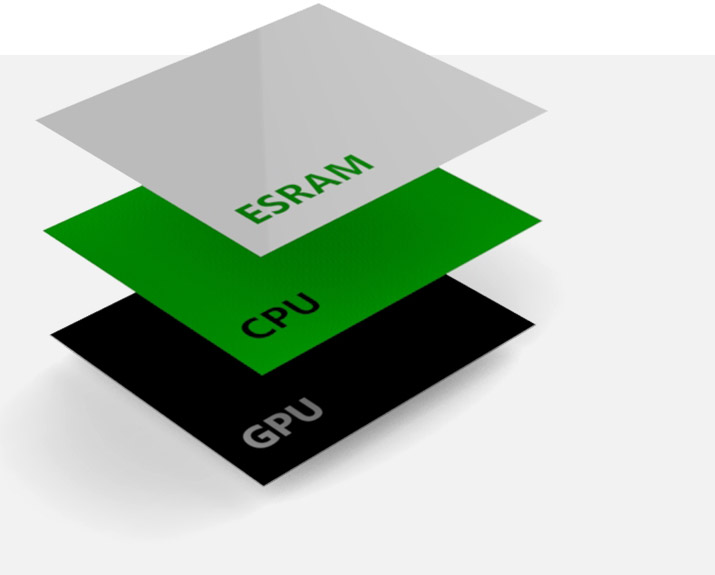
Vgleaks has a wealth of info, likely supplied from game developers with direct access to Xbox One specs, that looks to be very accurate at this point. According to their data, there’s roughly 50GB/s of bandwidth in each direction to the SoC’s embedded SRAM (102GB/s total bandwidth). The combination of the two plus the CPU-GPU connection at 30GB/s is how Microsoft arrives at its 200GB/s bandwidth figure, although in reality that’s not how any of this works. If it’s used as a cache, the embedded SRAM should significantly cut down on GPU memory bandwidth requests which will give the GPU much more bandwidth than the 256-bit DDR3-2133 memory interface would otherwise imply. Depending on how the eSRAM is managed, it’s very possible that the Xbox One could have comparable effective memory bandwidth to the PlayStation 4. If the eSRAM isn’t managed as a cache however, this all gets much more complicated.
| Microsoft Xbox One vs. Sony PlayStation 4 Memory Subsystem Comparison | ||||||||||||||
| Xbox 360 | Xbox One | PlayStation 4 | ||||||||||||
| Embedded Memory | 10MB eDRAM | 32MB eSRAM | - | |||||||||||
| Embedded Memory Bandwidth | 32GB/s | 102GB/s | - | |||||||||||
| System Memory | 512MB 1400MHz GDDR3 | 8GB 2133MHz DDR3 | 8GB 5500MHz GDDR5 | |||||||||||
| System Memory Bus | 128-bits | 256-bits | 256-bits | |||||||||||
| System Memory Bandwidth | 22.4 GB/s | 68.3 GB/s | 176.0 GB/s | |||||||||||
There are merits to both approaches. Sony has the most present-day-GPU-centric approach to its memory subsystem: give the GPU a wide and fast GDDR5 interface and call it a day. It’s well understood and simple to manage. The downsides? High speed GDDR5 isn’t the most power efficient, and Sony is now married to a more costly memory technology for the life of the PlayStation 4.
Microsoft’s approach leaves some questions about implementation, and is potentially more complex to deal with depending on that implementation. Microsoft specifically called out its 8GB of memory as being “power friendly”, a nod to the lower power operation of DDR3-2133 compared to 5.5GHz GDDR5 used in the PS4. There are also cost benefits. DDR3 is presently cheaper than GDDR5 and that gap should remain over time (although 2133MHz DDR3 is by no means the cheapest available). The 32MB of embedded SRAM is costly, but SRAM scales well with smaller processes. Microsoft probably figures it can significantly cut down the die area of the eSRAM at 20nm and by 14/16nm it shouldn’t be a problem at all.
Even if Microsoft can’t deliver the same effective memory bandwidth as Sony, it also has fewer GPU execution resources - it’s entirely possible that the Xbox One’s memory bandwidth demands will be inherently lower to begin with.


245 Comments
View All Comments
xaml - Thursday, May 23, 2013 - link
If every third Xbox 360 user had to get at least one repaired and after that died, bought a new one until finally salvaged by the 'Slim'...Niabureth - Wednesday, May 29, 2013 - link
And just how do you expect them to do that? Decisions on what hardware to use was made a lot earlier than Sony's PS4 presentation, meaning that train has already left the station. I'm guessing AMD is massproducing the hardware by now. Mircosoft: Oh we saw that Sony is going for a much more powerful architecture and we don't want any of the million of APU's u've just produced for us!JDG1980 - Wednesday, May 22, 2013 - link
If AMD is using Jaguar here, isn't that basically an admission that Bulldozer/Piledriver is junk, at least for gaming/desktop usage? Why don't they use a scaled-up Jaguar in their desktop APUs instead of Piledriver? The only thing Bulldozer/Piledriver seems to be good for is very heavily threaded loads - i.e. servers. Most desktop users are well served by even 4 cores, and it looks like they've already scaled Jaguar to 8. And AMD is getting absolutely killed on the IPC front on the desktop - if Jaguar is a step in the right direction then by all means it should be taken. BD/PD is a sunk cost, it should be written off, or restricted to Opterons only.tipoo - Wednesday, May 22, 2013 - link
Too big.Slaimus - Wednesday, May 22, 2013 - link
Bulldozer/Piledriver needs SOI. Steamroller is not ready yet, and it is not portable outside of Globalfoundries gate-first 28nm architecture. Jaguar is bulk 28nm and gate-last, which can be made by TSMC in large quantities at lower cost per wafer.JDG1980 - Wednesday, May 22, 2013 - link
All the more reason for AMD to switch to Jaguar in their mass-market CPUs and APUs.I'd be willing to bet money that a 4-core Jaguar clocked up to 3 GHz would handily beat a 4-module ("8-core") Piledriver clocked to 4 GHz. BD/PD is AMD's Netburst, a total FAIL of an architecture that needs to be dropped before it takes the whole company down with it.
Exophase - Wednesday, May 22, 2013 - link
Jaguar can't be clocked at 3GHz - 2GHz is closer to the hard limit as far as we currently know. It's clock limited by design, just look at the clock latency of FPU operations. IPC is at best similar to Piledriver (in practice probably a little worse), so in tasks heavily limited by single threaded performance Jaguar will do much worse. Consoles can bear limited single threaded performance to some extent but PCs can't.Spunjji - Wednesday, May 22, 2013 - link
It's effectively a low-power optimised Athlon 64 with added bits, so it's not going to scale any higher than Phenom did. That already ran out of steam on the desktop. Bulldozer/Piledriver may not have been the knockout blow AMD needed but they're scaling better than die-shrinking the same architecture yet again would have.JDG1980 - Wednesday, May 22, 2013 - link
Bobcat/Jaguar is a new architecture specifically designed for low-power usage. It's not the same as the K10 design, though it wouldn't surprise me if they did share some parts.And even just keeping K10 with tweaks and die-shrinks would have worked better on the desktop than the Faildozer series. Phenom II X6 1100T was made on an outdated 45nm process, and still beat the top 32nm Bulldozer in most benchmarks. A die-shrink to 28nm would not only be much cheaper to manufacture per chip than Bulldozer/Piledriver, but would perform better as well. It's only pride and the refusal to admit sunk costs that has kept AMD on their trail of fail.
kyuu - Wednesday, May 22, 2013 - link
That's a nice bit of FUD there. K10 had pretty much been pushed as far as it was going to go. Die-shrinking and tweaking it was not going to cut it. AMD needed a new architecture.Piledriver already handily surpasses K10 in every metric, including single-threaded performance.