Haswell GT3e Pictured, Coming to Desktops (R-SKU) & Notebooks
by Anand Lal Shimpi on April 10, 2013 7:21 PM EST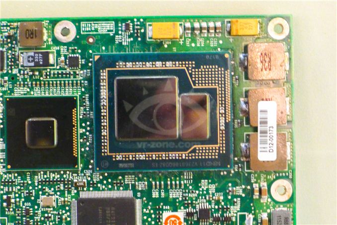
One of the worst kept secrets is Haswell will have four different GPU configurations: GT1, GT2, GT3 and GT3e. As with Sandy Bridge and Ivy Bridge, higher numbers mean more execution units, with GT3 topping out at 40 EUs. The lowercase e denotes an embedded DRAM part, with some amount of DRAM on the Haswell package itself (not on-die).
In an awesome scoop, the folks at VR-Zone managed to snag a photo of what looks like a quad-core Haswell die with GT3e graphics. The small package to the left should be the Lynx Point chipset (8-series), while the dual-die package on the right is Haswell + DRAM. The big square die should be Haswell itself with its 40 EU GPU, while the smaller die is the DRAM itself.
Intel hasn't officially acknowledged the existence of GT3e, but it did demonstrate performance of the part at CES earlier this year - targeting somewhere around the speed of NVIDIA's GeForce GT 650M. The DRAM size, operating frequency and bus width are all unknown at this point. I've heard the DRAM itself should be relatively small (~128MB), looking at the chip shot we get some indication but there's no confirmation of the specific type of memory we're looking at here (which obviously impacts die area).
Haswell GT3e will be available both in notebooks and desktops, however neither will come in socketed form (BGA-only). The desktop parts will carry an R suffix. This will be the beginning of Intel's socketed/soldered strategy on the desktop, which as of now is set to work sort of like tick tock - with the first chips on any new process being sold exclusively in BGA packages. Haswell will have socketed desktop SKUs, Broadwell won't, Skylake will, etc...
GT3e use in notebooks will be limited to larger designs it seems. Don't expect to find this level of graphics performance in a low wattage Ultrabook part, but it will likely surface in bigger notebooks - perhaps those driving ultra high resolution panels.
Source: VR Zone


64 Comments
View All Comments
ShieTar - Thursday, April 11, 2013 - link
Just looking at Anandtechs own bench comparison ( http://www.anandtech.com/bench/Product/580?vs=622 ) shows a difference between HD4000 and a 650M of a factor 3 to 4 in most games. Now if Haswell does nothing else besides going from 16 to 40 EUs, it is already making up a factor of 2.5. So if you allow that INTEL will also manage to improve efficiency and driver quality by a good deal, the 650M is definitely the level of performance that GT3 aims for.tipoo - Thursday, April 11, 2013 - link
I thought Intel themselves were saying "up to double" the performance of the HD4000. It wasn't clear if that was the GT3 with or without the eDRAM, but why have the number of the second lowest end chip as the "up to"?krumme - Thursday, April 11, 2013 - link
Agree, but that asumes the driver development will be there. Also for more than the most popular games, and as times moves on.Intels history shows, that it excactly them to show this will be the case. The old HD series is abandoned for driver support, the Atom line was abonned nearly before it hit market. Its a mess, and they leave customers with relatively far worse products than they bought.
Secondly if Broadwell comes with an entire new arch, as we predict, what will happen with develpment for the existing HD arch?
I wouldnt bet a second as a consumer on Intel instead of Nvidia or AMD, that the driver support will be there, before they have proved it even over a generation change.
Perhaps i am angry because the resent HD3000 video bug giving me chopping 23.xxx. Even my old NV 8600m gs was better, and the quality on dxva also looked better. Not to mention to mention a dirt cheap e350 APU beats it hands down on such a simple thing as video. My HD4000 machines look good on both desktop and ultrabook with no chopping, but the discrete card still looks to have better visual quality on both video and games on the same setting.
I dont know why Intel absolutely want that top speed, instead of improving quality. Its far more important for their brand in the long run. They have a job to do.
But all in all, i hope its good because as the nerd i am i always change my gear each year, so i buy whatever they do :)
TempestDash - Thursday, April 11, 2013 - link
Put this into an NUC and I'll be yours forever, Intel.Shadowmaster625 - Thursday, April 11, 2013 - link
This whole non-socketed strategy is going to fial in Intel's face. Dont forget that intel isnt jsut screwing the consumer here, Intel is gouging the oems too. What happens when they handle RMA's? 100 or 1000 motherboards a day or whatever the rate is for that sort of repair. That means they have to do something with 100 or 1000 cpus a day, or just throw them away. I'm sure many will get thrown away. But what will they do with them even if they keep them? It becomes a big money sucking pain in the butt process, costing millions of dollars. It is just going to make the PC industry implode faster, and intel right along with it.MrSpadge - Thursday, April 11, 2013 - link
I suspect it's rather the OEMs pushing for this, to save a few bucks per system.. and to sell more systems down the road (motherboard fails after warrenty, which you'd by now just replace).UpSpin - Thursday, April 11, 2013 - link
How often did a CPU or motherboard fail for you? How often does a normal person replace the CPU or motherboard only. And how were OEMs able to handle all those notebooks, ultrabooks, tablets, all-in one systems which don't have a socket since several years. And why is the smartphone / tablet market one of the most profitable ones, yet they have everything integrated on a single board?MrSpadge - Thursday, April 11, 2013 - link
To me it would sound lovely to use the eDRAM as a L4 cache for the number-crunching CPU!tipoo - Thursday, April 11, 2013 - link
I wonder if it can be used like that? Is it dynamically split between CPU and GPU if the GPU isn't using it?MrSpadge - Friday, April 12, 2013 - link
So far I've heard it's for the GPU only. It might be accessible through OpenCL, but the overhead might kill any performance gains over main memory. It would seem akward, though, to restrict its usage to the GPU, since the CPU sits right besides it and the ring bus could surely handle some more load. It could be an issue of unifying GPU and CPU adress space - a point Intel has not quite reached, to my knowledge.