NVIDIA Tegra 4 Architecture Deep Dive, Plus Tegra 4i, Icera i500 & Phoenix Hands On
by Anand Lal Shimpi & Brian Klug on February 24, 2013 3:00 PM ESTThe GPU
Tegra 4 features an evolved GPU core compared to Tegra 3. The architecture retains a fixed division between pixel and vertex shader hardware, making it the only modern mobile GPU architecture not to adopt a unified shader model.
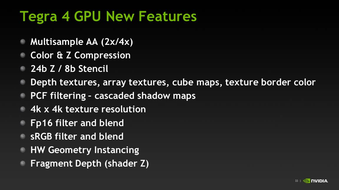

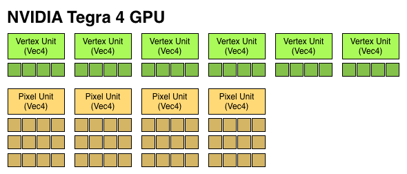
I already described a lot of what makes the Tegra 4 GPU different in our original article on the topic. The diagram below gives you an idea of how the pixel and vertex shader hardware grew over the past 3 generations:
We finally have a competitive GPU architecture from NVIDIA. It’s hardly industry leading in terms of specs, but there’s a good amount of the 80mm^2 die dedicated towards pixel and vertex shading hardware. There's also a new L2 texture cache that helps improve overall bandwidth efficiency.
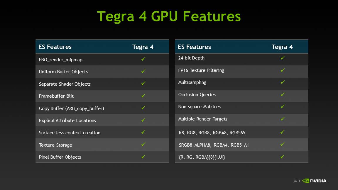
The big omission here is the lack of full OpenGL ES 3.0 support. NVIDIA’s pixel shader hardware remains FP24, while the ES 3.0 spec requires full FP32 support for both pixel and vertex shaders. NVIDIA also lacks ETC and FP texture support, although some features of ES 3.0 are implemented (e.g. Multiple Render Targets).
| Mobile SoC GPU Comparison | |||||||||||||||
| GeForce ULP (2012) | PowerVR SGX 543MP2 | PowerVR SGX 543MP4 | PowerVR SGX 544MP3 | PowerVR SGX 554MP4 | GeForce ULP (2013) | ||||||||||
| Used In | Tegra 3 | A5 | A5X | Exynos 5 Octa | A6X | Tegra 4 | |||||||||
| SIMD Name | core | USSE2 | USSE2 | USSE2 | USSE2 | core | |||||||||
| # of SIMDs | 3 | 8 | 16 | 12 | 32 | 18 | |||||||||
| MADs per SIMD | 4 | 4 | 4 | 4 | 4 | 4 | |||||||||
| Total MADs | 12 | 32 | 64 | 48 | 128 | 72 | |||||||||
| GFLOPS @ Shipping Frequency | 12.4 GFLOPS | 16.0 GFLOPS | 32.0 GFLOPS | 51.1 GFLOPS | 71.6 GFLOPS | 74.8 GFLOPS | |||||||||
For users today, the lack of OpenGL ES 3.0 support likely doesn’t matter - but it’ll matter more in a year or two when game developers start using OpenGL ES 3.0. NVIDIA is fully capable of building an OpenGL ES 3.0 enabled GPU, and I suspect the resistance here boils down to wanting to win performance comparisons today without making die size any larger than it needs to be. Remembering back to the earlier discussion about NVIDIA’s cost position in the market, this decision makes sense from NVIDIA’s stance although it’s not great for the industry as a whole.
Tegra 4i retains the same base GPU architecture as Tegra 4, but dramatically cuts down on hardware. NVIDIA goes from 4 down to 3 vertex units, and moves to two larger pixel shader units (increasing the ratio of compute to texture hardware in the T4i GPU). The max T4i GPU clock drops a bit down to 660MHz, but that still gives it substantially more performance than NVIDIA’s Tegra 3.
Memory Interface
The first three generations of Tegra SoCs had an embarrassingly small amount of memory bandwidth, at least compared to Apple, Samsung and Qualcomm. Admittedly, Samsung and Qualcomm were late adopters of a dual-channel memory interface, but they still got there much quicker than NVIDIA did.
With Tegra 4, complaints about memory bandwidth can finally be thrown out the window. The Tegra 4 SoC features two 32-bit LPDDR3 memory interfaces, bringing it up to par with the competition. The current max data rate supported by Tegra 4’s memory interfaces is 1866MHz, but that may go up in the future.
Tegra 4 won’t ship in a PoP (package-on-package) configuration and will have to be paired with external DRAM. This will limit Tegra 4 to larger devices, but it should still be able to fit in a phone.
Unfortunately, Tegra 4i only has a single channel LPDDR3 memory interface. Tegra 4i on the other hand will be available in PoP as well as discrete configurations. The PoP configuration may top out at LPDDR3-1600, while the discrete version can scale up to 1866MHz and beyond.


75 Comments
View All Comments
PingviN - Monday, February 25, 2013 - link
Tegra made an operating loss of $150 million for fiscal year 2012, despite getting into both the Nexus 7 (the refresh coming this year has been lost to Qualcomm) and the Surface RT. Sales prognosis cut almost in half for the fiscal year 2013. To date, Nvidia hasn't had any profit coming out of Tegra and now it's in limbo mode until Tegra 4 is released because Tegra 3 gets smashed by it's competition.It's been a pretty crappy year for Tegra.
guilmon14 - Tuesday, February 26, 2013 - link
I don't know anything about this company "tegra", but have you heard about Nvidia? I heard they're doing great!http://nvidianews.nvidia.com/Releases/NVIDIA-Repor...
According to this Nvidia is up in income, revenue, and equity.
If you wanted to check the easy way just look at nvidia's wikipedia page, gives you all the nice money numbers.
http://en.wikipedia.org/wiki/Nvidia
trajan2448 - Monday, February 25, 2013 - link
5 years down the road phones will be cooking our dinner. It's amazing how fast the tech is advancing now.Scannall - Monday, February 25, 2013 - link
If they don't hustle right along, SOC's with the PowerVR 6 series (Rogue) will beat them to market. And considering their GPU just barely squeaks by the iPad as it is, it will be behind early on.Khato - Monday, February 25, 2013 - link
Was it specifically stated that the Tegra 4 SPECint/W figure was running on the high speed cores? As is mentioned later on the page, a SPECint2000 of 520 is within reach of the power optimized companion core, so the only reason I'd expect NVIDIA to not use the companion core for this data is if they explicitly stated that it wasn't.Part of the cause for my suspicion is that the Power vs DMIPS chart that Samsung recently provided for the Exynos 5 Octa shows 8k DMIPS at 1 watt... and from the press coverage back in 2009 for the A9 hard macros there's both the 10k DMIPS at 1.9 watts and 2GHz with the speed speed optimized and 4k DMIPS at 250 mW and 800 MHz for the power optimized. Which equate to 5.26 DMIPS/mW and 8 DMIPS/mW, respectively. Now the 2GHz data point should be even worse off than Tegra 3 and yet it only shows the Samsung Exynos 5 Octa as being 52% more efficient.
Going into estimating rather than published numbers, if we up the efficiency of Tegra 3 a bit compared to that 2GHz figure then it's likely going to be closer to A15 being 30% more efficient... which you then add the known ~40% efficiency bump going from a performance to power implementation and you get the kind of drastic increase NVIDIA is touting.
Wilco1 - Monday, February 25, 2013 - link
It doesn't matter whether they used the 5th core or one of the fast ones. By definition the cross over point is where the 5th core uses as much power as a fast core. Since that is ~800MHz, the power efficiency is the same. The 5th core can likely clock to well over 1GHz, but then it uses more power than a fast core.You are basically right that some of the 73% MIPS/W improvement comes from the 40-28nm process change. However the combined improvement of process and micro architecture means that you can use the low power core far more often. The 5th core in Tegra 4 is effectively more than 3 times as fast than the one in Tegra 3. So that means lots of tasks which needed 1-2 fast Tegra 3 cores can now run on the 5th Tegra 4 core. That means the power efficiency will actually improve by what NVidia suggests.
Khato - Monday, February 25, 2013 - link
Mind sharing the source for that? The wording in this article implies differently - "That 825MHz mark ends up being an important number, because that’s where the fifth companion Cortex A15 tops out at." Given 1.9GHz for the performance-optimized cores, something around 800 MHz sounds about right for the max frequency of a power-optimized version.Anyway, there's no question that Tegra 4 will be quite a bit more power efficient simply by virtue of being able able to run more workloads exclusively on the companion core. As said before, in exchange for a much lower cap on maximum frequency a power optimized synthesis gives at least a 40% bump in efficiency... and now that power optimized core will still deliver respectable performance.
Wilco1 - Monday, February 25, 2013 - link
Read http://www.nvidia.com/content/PDF/tegra_white_pape... it explains the difference between leakage and active power on low power and high performance transistors. It explicitly says the 5th core in Tegra is capped at 500MHz as that is where it is as power efficient as a fast core. The graphs and the word capped suggest the 5th core can go faster but there is no point.Note that Tegra 3 uses a different process with low power transistors for the 5th core rather than a low power synthesis (not that they couldn't have done that too, but it is never mentioned and the 5th core looks pretty much the same in the die plots). I presume Tegra 4 does the same on the 28nm process.
Khato - Tuesday, February 26, 2013 - link
Okay, so your commentary is based on the Tegra 3 which is using an entirely different approach to power savings for the companion core. Note that all of the data I was referencing for the difference in efficiency between ARM's two A9 hard macros was on the same process and hence is more applicable to the case of Tegra 4. As you correctly state, Tegra 3 gains its power efficiency for the companion core by using the LP process rather than a low power synthesis, likely due to it being a simpler and faster route to the desired end result and equally effective for their design goals.Tegra 4 isn't playing process games for the companion core. How do you gain efficiency on the same process? You loosen timings to allow for the usage of smaller transistors, less flop stages, so on so forth. The end result being that you sacrifice maximum switching speed to reduce both leakage and dynamic power. From all the information that NVIDIA has made available it's a completely different implementation from Tegra 3.
Wilco1 - Tuesday, February 26, 2013 - link
Tegra 4 does exactly the same as Tegra 3. According to NVidia's white paper on Tegra 4 (http://www.nvidia.com/docs/IO/116757/NVIDIA_Quad_a... it also uses low power transistors for the 5th core. Again if you look at the die photos of Tegra 4 all 5 cores are identical just like Tegra 3. So that seems to exclude a different synthesis.The way NVidia get a low power core is by using low power transistors. TSMC 28nm process supports several different transistor libraries, from high performance high leakage to low performance low leakage. Based on the information we have all they have done is swap the transistor libraries.