NVIDIA Tegra 4 Architecture Deep Dive, Plus Tegra 4i, Icera i500 & Phoenix Hands On
by Anand Lal Shimpi & Brian Klug on February 24, 2013 3:00 PM ESTSilicon makers almost always put together a reference design of their own for both testing their hardware, optimizing software stack, and generally having something to build to. Increasingly we’ve seen these vendors then take that reference design and do something with it beyond just having it for their own internal use — after all, if you’ve built and qualified a device, it makes sense to do something with it. While NVIDIA isn’t going to sell the FFRD directly, it’s a platform they can quickly hand off to OEMs wanting to implement a smartphone-platform with Tegra 4 or 4i relatively quickly.
To that end, NVIDIA has crafted Phoenix, which is their very own FFRD (Form Factor Reference Design) for both Tegra 4 and 4i versions. The high level specifications are what you’d expect for something from this current generation, with a 5-inch 1080p display, LTE, relatively thin profile, and of course a Tegra 4 SoC inside.
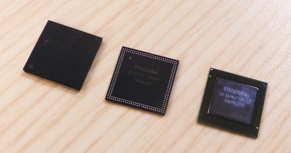
There are actually three different versions of the Phoenix — one in a version with Tegra 4, Tegra 4i without PoP (an external DRAM package), and a Tegra 4i version with PoP memory. All of them have the same PCB geometry inside, just a different SoC, and in the case of the Tegra 4 version, an external Icera i500 modem. NVIDIA showed us an image of their Tegra 4 Phoenix PCB, and in addition the Tegra 4i non PoP and Tegra 4 PCBs in the flesh. The Tegra 4 version has to include both Icera i500 and a MCP DRAM plus NAND of its own adjacent to it, right next to the DRAM for the Tegra 4. On the Tegra 4i version there’s simply unused space in the region occupied by those packages.
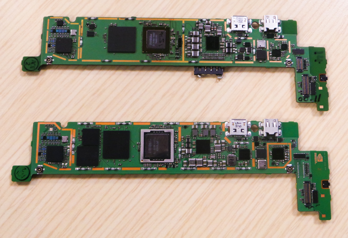
Glancing at the Tegra 4i package, we can also get Grey’s actual internal codename, which isn’t T30 series or T40 but rather T8A. The rest of the platform is basically what you’d expect for a modern device, and the PCB follows the rather typical L shaped design that’s common right now across the entire segment.


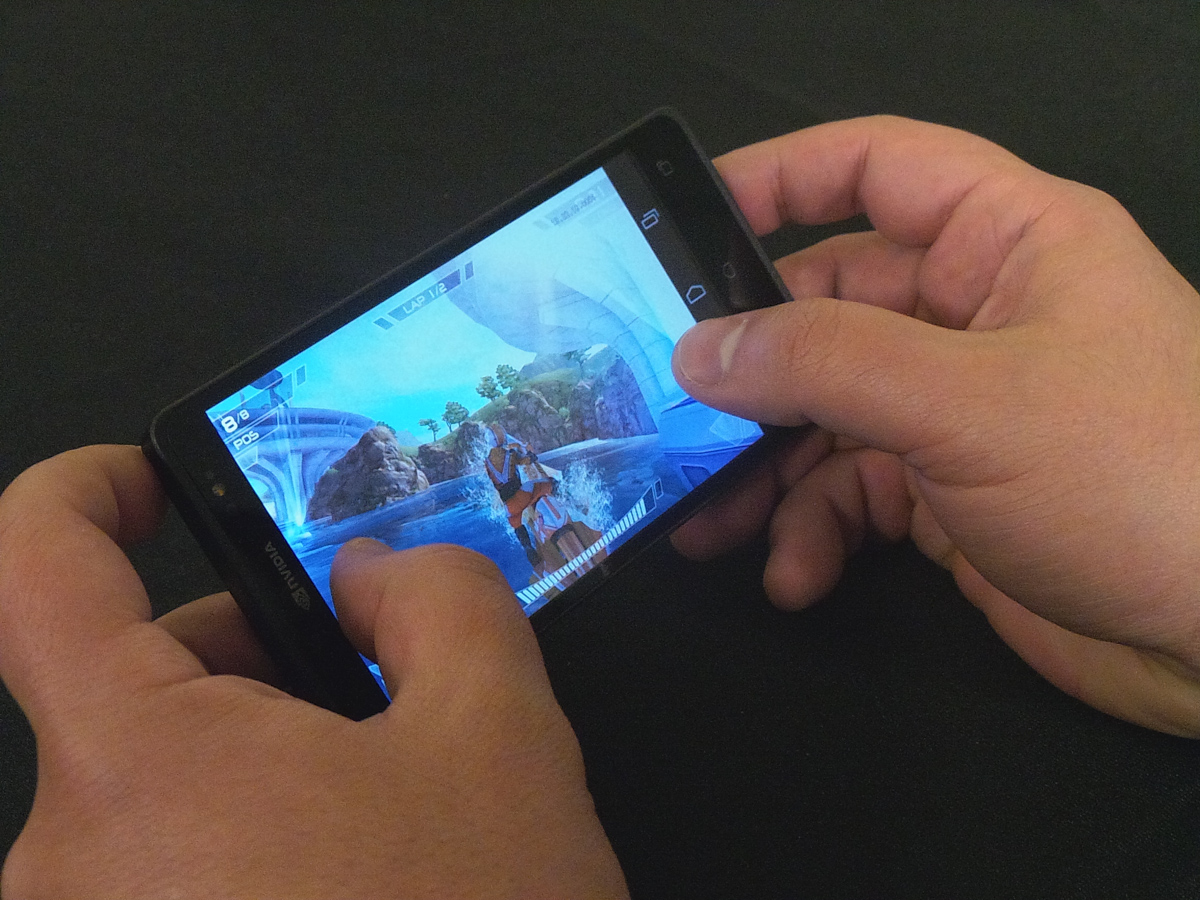
NVIDIA also showed a Tegra 4i based version of the Phoenix playing a version of Riptide 2 at 1080p with even more graphical assets (real time lighting, shadows, and improved water simulation) enabled over the previous version of Riptide optimized for Tegra 3.
I didn’t get too much time to play with the Phoenix – like any reference design from any of the players in this space it’s more of a function over form piece of equipment for developers or the silicon vendor themselves to get easy access to the insides – but superficially it’s the right kind of stuff for a smartphone right now.


75 Comments
View All Comments
klmccaughey - Sunday, February 24, 2013 - link
Definitely. All good for us too! :)twotwotwo - Sunday, February 24, 2013 - link
> In the PC industry we learned that there’s no real downside to quad-core as long as you can power gate individual cores, and turbo up to higher frequencies when fewer than four cores are active, there’s no real tradeoff other than cost.I'm not completely sure, because there are always other possible uses for die area.
You could do the big/little thing with A7 'companion' cores, like Samsung. You could use even more area for GPU, like Apple. Wiki suggests you could double the L2 cache to 4MB (though more cache would always be eating power, even with only one core turned on).
But in favor of quad-core: software might start using cores a little more effectively w/time--Google and Apple are apparently trying to make WebKit able to do things like HTML parsing and JavaScript garbage collection in the background, and Microsoft's browser team backgrounds JavaScript compilation. And the other uses of space are also only sort-of useful, and cores (like GHz) are handy for marketing. I can't say I know what the right tradeoff for NVidia is, only that there were were other seemingly-interesting options.
guidryp - Sunday, February 24, 2013 - link
"there are always other possible uses for die area"Yes, in the case of Tegra 3, they could certainly have used extra GPU power more than 4 CPU cores. But they seem to have remedied that this time.
twotwotwo - Monday, February 25, 2013 - link
Def possible, and what they disclosed in this presentation would suggest they've handled it.All that's working against them, GPU-wise, is that user expectations increased since last gen, and Mali/PowerVR improved. So now T4i needs to drive 1080p phone screens and T4 needs to drive screens like the Nexus 10's, if they want to be the most bleeding-edge, anyway.
But they did talk about large integer-factor improvements in the GPU, so maybe they haven't merely built the GPU that would've been nice to have last gen, but moved up enough to be great this gen.
sosadsohappy - Sunday, February 24, 2013 - link
Samsung has just said it is doing A15-A7 pairing. Saying out the future plans just to keep the crowd excited is not new. That does not rule out the possibility of Qualcomm or Nvidia going for similar big.LITTLE designs. They are for the next-gen I would think. (Tell me if I am wrong but have anyone sampled big.LITTLE based SoC yet?)And talking about die area, what is impressive about Nvidia is how their chips are always smaller. Quad-core A15 is about 80mm^2 while you can check for the sizes of Qualcomm's or Apple's chips! FWIW Apple's are not in 28nm but still they don't scale equally.
I am excited to see the 60mm^2 (right?) chip (Tegra4i). If it is what they claim, it should have great battery life for a smartphone.
s44 - Monday, February 25, 2013 - link
4+1 is Nvidia's version of big.LITTLE. The 1 low-power A15 is about the same die space as the 4 A7s on the next Exynos...sosadsohappy - Monday, February 25, 2013 - link
Yes. The only difference is that the big.LITTLE will sport different architectures on the big and LITTLE while NV's 4+1 will have the same arch (A15 for both).And personally I think 4+1 is better as of now until we have Atlas and Apollo combination of big.LITTLE because (correct me if I'm wrong) A7 does not have as much of memory parallelism, it is to weak as well...
No matter what, it has been impressive that Nvidia chips have significantly lower die size than the competition's dual-core chips!
Krysto - Monday, February 25, 2013 - link
Too weak? For what? Receiving notifications? We'll see if Tegra 4 is more energy efficient than Samsung's Exynos 5 Octa later this year. Then we might get a better idea whether Nvidia or ARM's implementation is better.And I agree. Nvidia managed to have the same graphics performance + a quad core Cortex A15 CPU in 80mm2 vs Apple with a dual core CPU and same graphics performance in 120 mm2. That's pretty impressive, even if it arrives half a year late.
I still wish Nvidia would actually want to compete at the high-end though, with a 120mm2 chip, and beat Apple. It annoys me that they are still trying to build only "good enough for most people" chips. They should be trying to be the king of mobile graphics. They are freaking Nvidia, and they can't even beat a mobile GPU maker? Come on, Nvidia.
name99 - Monday, February 25, 2013 - link
> In the PC industry we learned that there’s no real downside to quad-core as long as you can power gate individual cores, and turbo up to higher frequencies when fewer than four cores are active, there’s no real tradeoff other than cost.Sony Ericsson recently released a paper claiming this was not true, even apart from the die area issues. In particular they claimed that with current technology, coupling capacitance, ground plane issues, communication (with the L2, including coherence) and suchlike, quad-core imposed something like a 25% reduction in peak MHz possible for two cores, compared to those same two cores isolated rather than on a quad-core die.
Now obviously any company publication is talking up its book, but I imagine they're not going to make a statement that is blatantly false in a technical publication, implying there is some truth to what they say.
Wilco1 - Wednesday, February 27, 2013 - link
Given Tegra 4i achieves 2.3GHz in a quad core with shared L2, way more than Krait which uses per-CPU L2, I think the claim that a shared L2 is clock limiting seems more marketing than substance.