NVIDIA Tegra 4 Architecture Deep Dive, Plus Tegra 4i, Icera i500 & Phoenix Hands On
by Anand Lal Shimpi & Brian Klug on February 24, 2013 3:00 PM ESTNVIDIA has upped its ISP game with Tegra 4, and includes the same ISP in both Tegra 4 and 4i, which they’ve dubbed Chimera. This new ISP includes a number of features which were already demonstrated at CES, but NVIDIA went into greater detail.

NVIDIA’s major new feature with Tegra 4 is inclusion of new APIs which leverage the GPU to enable computational camera features In addition to the traditional ISP pipeline. To begin, NVIDIA has made their own enhancements in the imaging chain which leverage this GPU-assisted architecture that sits atop the normal ISP. They’ve outlined a few features which work atop this — HDR panorama, HDR stills, and real time object tracking. The end result is that Chimera is one part programming model and APIs for future development efforts by third parties, another part first party software that NVIDIA will distribute for integration in OEM cameras which includes the HDR features and object tracking.
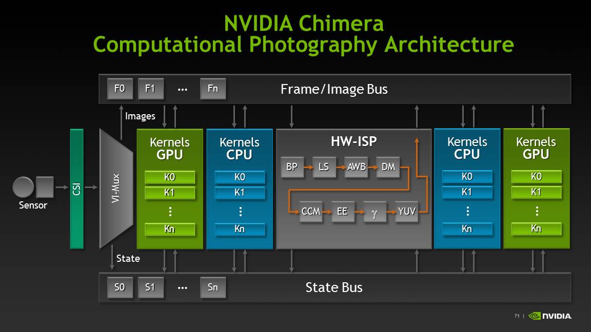
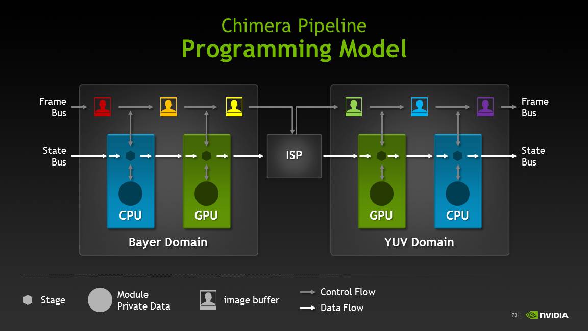
Chimera allows developers to build blocks around the traditional ISP data flow and get to manipulate either bayer image data or YUV space image data on the CPU or GPU using their own framework. There are still a lot of details to come about the programming model and how this will be exploited, but there clearly is space here for NVIDIA to try and make a case for their GPU being useful for image processing. At the same time, the elephant in the room is OpenCL (and its current absence on Tegra 4) and what direction the industry will take that to leverage GPU compute for some computational photography processing.
The novel new feature of note is something I was skeptical about upon seeing at CES — single frame HDR video. The traditional route for HDR video capture is to capture at twice the framerate of the intended output video, for example for 720p30 video with a two-frame HDR, that would mean capture at 720p60 with two different exposures. What NVIDIA does is a bit different. Instead of capturing two exposures and combining them after capture, NVIDIA has found a way to drive selected CMOS sensors (both IMX135 from Sony and AR0833 from Aptina have been called out specifically, but there are more) in some special fashion, and recombine interleaved high and low exposure images (the +1 stop, –1 stop) image into one equivalent frame. This is all done on the GPU using the same Chimera pipeline blocks, but with NVIDIA’s own algorithm. The results are actually pretty impressive, NVIDIA claims 3 stops of dynamic range (~24 dB), and no recombination artifacts.
Previous demonstrations of HDR video capture on a few other platform have had halos around moving elements because of the issues associated with taking two temporally different frames and recombining them. With NVIDIA’s HDR video capture I saw no halos even on very fast moving objects, with the same quality of HDR.
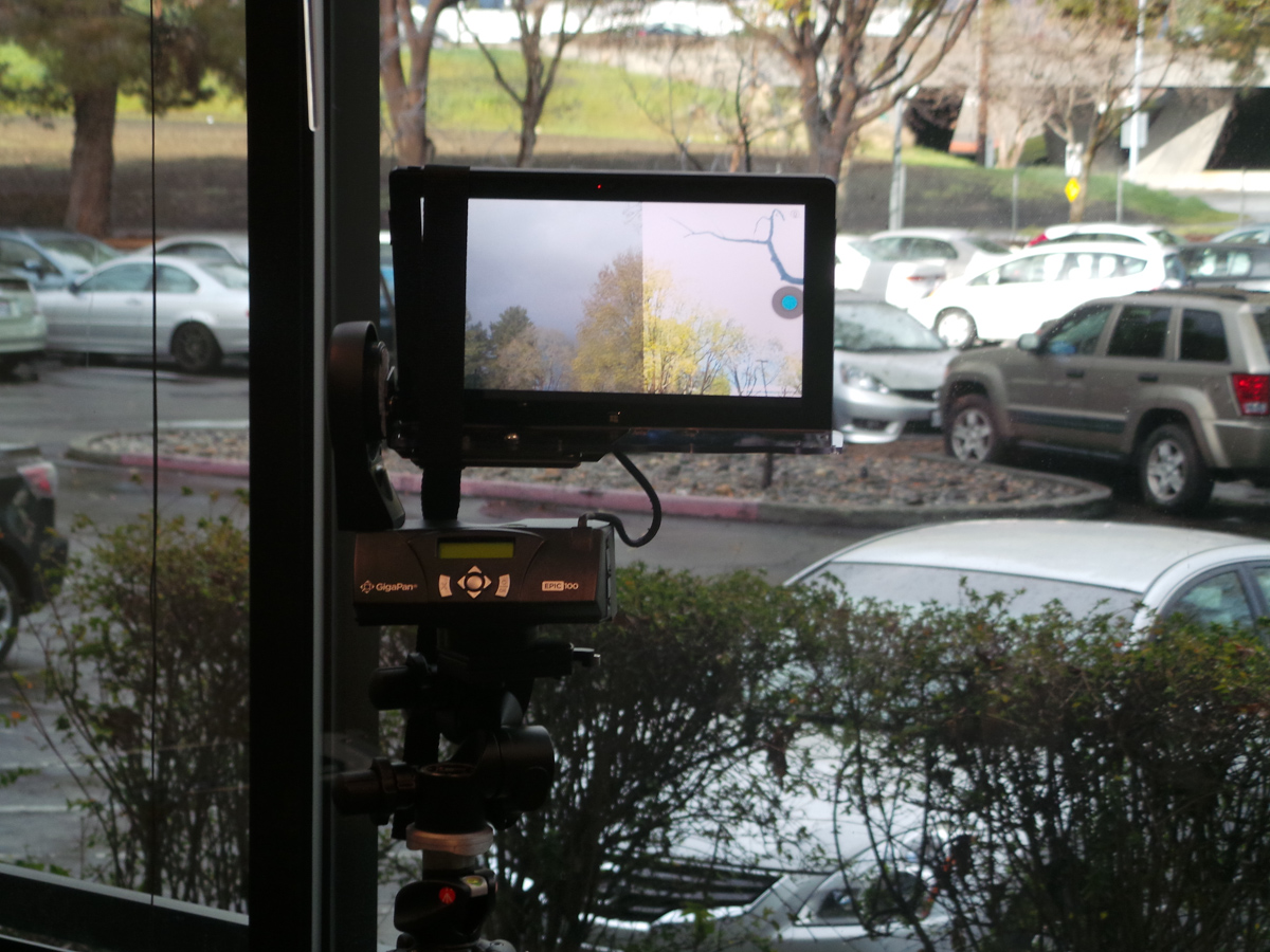
NVIDIA also demonstrated their panorama capture which includes HDR as well, using a GigaPan Epic 100. Admittedly a better demo might be hand held to demonstrate how well the ISP is able to compensate for change in perspective from the tablet moving around in the hand, the resulting image was the same quality of HDR as the still however. I also saw object tracking which essentially is face tracking (and thus AE / AF assist to that subject) but taken to arbitrary subjects. Paint a box around the object you want to track, and the camera will perform feature extraction and machine learn a model around the object. Rotating around complex geometries seemed to work decently well — the model learns slowly so slow movements can be accommodated, faster moving subjects might not be object tracked.

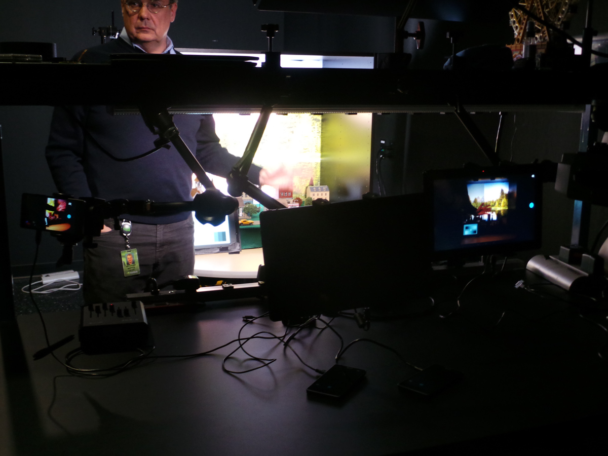
I also got a chance to tour NVIDIA’s camera tuning labs, where they characterize smartphone CMOSes for handset markers, and work with them on tuning their ISP and imaging experience. I saw one calibration room with many different scenes, and then another room with large test charts, and two sets of standard test scenes in lightboxes. The ever-familiar GMB color checker card and ISO12233 charts were everywhere as well.


75 Comments
View All Comments
klmccaughey - Sunday, February 24, 2013 - link
Definitely. All good for us too! :)twotwotwo - Sunday, February 24, 2013 - link
> In the PC industry we learned that there’s no real downside to quad-core as long as you can power gate individual cores, and turbo up to higher frequencies when fewer than four cores are active, there’s no real tradeoff other than cost.I'm not completely sure, because there are always other possible uses for die area.
You could do the big/little thing with A7 'companion' cores, like Samsung. You could use even more area for GPU, like Apple. Wiki suggests you could double the L2 cache to 4MB (though more cache would always be eating power, even with only one core turned on).
But in favor of quad-core: software might start using cores a little more effectively w/time--Google and Apple are apparently trying to make WebKit able to do things like HTML parsing and JavaScript garbage collection in the background, and Microsoft's browser team backgrounds JavaScript compilation. And the other uses of space are also only sort-of useful, and cores (like GHz) are handy for marketing. I can't say I know what the right tradeoff for NVidia is, only that there were were other seemingly-interesting options.
guidryp - Sunday, February 24, 2013 - link
"there are always other possible uses for die area"Yes, in the case of Tegra 3, they could certainly have used extra GPU power more than 4 CPU cores. But they seem to have remedied that this time.
twotwotwo - Monday, February 25, 2013 - link
Def possible, and what they disclosed in this presentation would suggest they've handled it.All that's working against them, GPU-wise, is that user expectations increased since last gen, and Mali/PowerVR improved. So now T4i needs to drive 1080p phone screens and T4 needs to drive screens like the Nexus 10's, if they want to be the most bleeding-edge, anyway.
But they did talk about large integer-factor improvements in the GPU, so maybe they haven't merely built the GPU that would've been nice to have last gen, but moved up enough to be great this gen.
sosadsohappy - Sunday, February 24, 2013 - link
Samsung has just said it is doing A15-A7 pairing. Saying out the future plans just to keep the crowd excited is not new. That does not rule out the possibility of Qualcomm or Nvidia going for similar big.LITTLE designs. They are for the next-gen I would think. (Tell me if I am wrong but have anyone sampled big.LITTLE based SoC yet?)And talking about die area, what is impressive about Nvidia is how their chips are always smaller. Quad-core A15 is about 80mm^2 while you can check for the sizes of Qualcomm's or Apple's chips! FWIW Apple's are not in 28nm but still they don't scale equally.
I am excited to see the 60mm^2 (right?) chip (Tegra4i). If it is what they claim, it should have great battery life for a smartphone.
s44 - Monday, February 25, 2013 - link
4+1 is Nvidia's version of big.LITTLE. The 1 low-power A15 is about the same die space as the 4 A7s on the next Exynos...sosadsohappy - Monday, February 25, 2013 - link
Yes. The only difference is that the big.LITTLE will sport different architectures on the big and LITTLE while NV's 4+1 will have the same arch (A15 for both).And personally I think 4+1 is better as of now until we have Atlas and Apollo combination of big.LITTLE because (correct me if I'm wrong) A7 does not have as much of memory parallelism, it is to weak as well...
No matter what, it has been impressive that Nvidia chips have significantly lower die size than the competition's dual-core chips!
Krysto - Monday, February 25, 2013 - link
Too weak? For what? Receiving notifications? We'll see if Tegra 4 is more energy efficient than Samsung's Exynos 5 Octa later this year. Then we might get a better idea whether Nvidia or ARM's implementation is better.And I agree. Nvidia managed to have the same graphics performance + a quad core Cortex A15 CPU in 80mm2 vs Apple with a dual core CPU and same graphics performance in 120 mm2. That's pretty impressive, even if it arrives half a year late.
I still wish Nvidia would actually want to compete at the high-end though, with a 120mm2 chip, and beat Apple. It annoys me that they are still trying to build only "good enough for most people" chips. They should be trying to be the king of mobile graphics. They are freaking Nvidia, and they can't even beat a mobile GPU maker? Come on, Nvidia.
name99 - Monday, February 25, 2013 - link
> In the PC industry we learned that there’s no real downside to quad-core as long as you can power gate individual cores, and turbo up to higher frequencies when fewer than four cores are active, there’s no real tradeoff other than cost.Sony Ericsson recently released a paper claiming this was not true, even apart from the die area issues. In particular they claimed that with current technology, coupling capacitance, ground plane issues, communication (with the L2, including coherence) and suchlike, quad-core imposed something like a 25% reduction in peak MHz possible for two cores, compared to those same two cores isolated rather than on a quad-core die.
Now obviously any company publication is talking up its book, but I imagine they're not going to make a statement that is blatantly false in a technical publication, implying there is some truth to what they say.
Wilco1 - Wednesday, February 27, 2013 - link
Given Tegra 4i achieves 2.3GHz in a quad core with shared L2, way more than Krait which uses per-CPU L2, I think the claim that a shared L2 is clock limiting seems more marketing than substance.