NVIDIA Tegra 4 Architecture Deep Dive, Plus Tegra 4i, Icera i500 & Phoenix Hands On
by Anand Lal Shimpi & Brian Klug on February 24, 2013 3:00 PM ESTThe GPU
Tegra 4 features an evolved GPU core compared to Tegra 3. The architecture retains a fixed division between pixel and vertex shader hardware, making it the only modern mobile GPU architecture not to adopt a unified shader model.
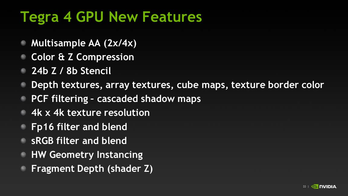

I already described a lot of what makes the Tegra 4 GPU different in our original article on the topic. The diagram below gives you an idea of how the pixel and vertex shader hardware grew over the past 3 generations:
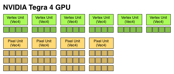
We finally have a competitive GPU architecture from NVIDIA. It’s hardly industry leading in terms of specs, but there’s a good amount of the 80mm^2 die dedicated towards pixel and vertex shading hardware. There's also a new L2 texture cache that helps improve overall bandwidth efficiency.
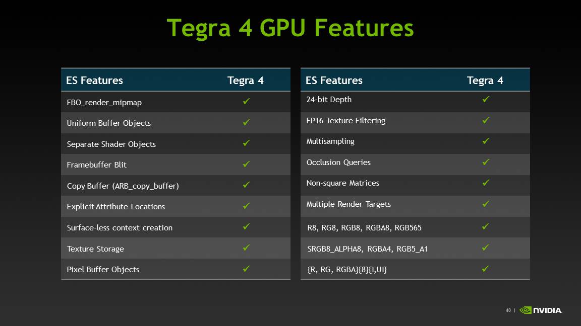
The big omission here is the lack of full OpenGL ES 3.0 support. NVIDIA’s pixel shader hardware remains FP24, while the ES 3.0 spec requires full FP32 support for both pixel and vertex shaders. NVIDIA also lacks ETC and FP texture support, although some features of ES 3.0 are implemented (e.g. Multiple Render Targets).
| Mobile SoC GPU Comparison | |||||||||||||||
| GeForce ULP (2012) | PowerVR SGX 543MP2 | PowerVR SGX 543MP4 | PowerVR SGX 544MP3 | PowerVR SGX 554MP4 | GeForce ULP (2013) | ||||||||||
| Used In | Tegra 3 | A5 | A5X | Exynos 5 Octa | A6X | Tegra 4 | |||||||||
| SIMD Name | core | USSE2 | USSE2 | USSE2 | USSE2 | core | |||||||||
| # of SIMDs | 3 | 8 | 16 | 12 | 32 | 18 | |||||||||
| MADs per SIMD | 4 | 4 | 4 | 4 | 4 | 4 | |||||||||
| Total MADs | 12 | 32 | 64 | 48 | 128 | 72 | |||||||||
| GFLOPS @ Shipping Frequency | 12.4 GFLOPS | 16.0 GFLOPS | 32.0 GFLOPS | 51.1 GFLOPS | 71.6 GFLOPS | 74.8 GFLOPS | |||||||||
For users today, the lack of OpenGL ES 3.0 support likely doesn’t matter - but it’ll matter more in a year or two when game developers start using OpenGL ES 3.0. NVIDIA is fully capable of building an OpenGL ES 3.0 enabled GPU, and I suspect the resistance here boils down to wanting to win performance comparisons today without making die size any larger than it needs to be. Remembering back to the earlier discussion about NVIDIA’s cost position in the market, this decision makes sense from NVIDIA’s stance although it’s not great for the industry as a whole.
Tegra 4i retains the same base GPU architecture as Tegra 4, but dramatically cuts down on hardware. NVIDIA goes from 4 down to 3 vertex units, and moves to two larger pixel shader units (increasing the ratio of compute to texture hardware in the T4i GPU). The max T4i GPU clock drops a bit down to 660MHz, but that still gives it substantially more performance than NVIDIA’s Tegra 3.
Memory Interface
The first three generations of Tegra SoCs had an embarrassingly small amount of memory bandwidth, at least compared to Apple, Samsung and Qualcomm. Admittedly, Samsung and Qualcomm were late adopters of a dual-channel memory interface, but they still got there much quicker than NVIDIA did.
With Tegra 4, complaints about memory bandwidth can finally be thrown out the window. The Tegra 4 SoC features two 32-bit LPDDR3 memory interfaces, bringing it up to par with the competition. The current max data rate supported by Tegra 4’s memory interfaces is 1866MHz, but that may go up in the future.
Tegra 4 won’t ship in a PoP (package-on-package) configuration and will have to be paired with external DRAM. This will limit Tegra 4 to larger devices, but it should still be able to fit in a phone.
Unfortunately, Tegra 4i only has a single channel LPDDR3 memory interface. Tegra 4i on the other hand will be available in PoP as well as discrete configurations. The PoP configuration may top out at LPDDR3-1600, while the discrete version can scale up to 1866MHz and beyond.


75 Comments
View All Comments
klmccaughey - Sunday, February 24, 2013 - link
Definitely. All good for us too! :)twotwotwo - Sunday, February 24, 2013 - link
> In the PC industry we learned that there’s no real downside to quad-core as long as you can power gate individual cores, and turbo up to higher frequencies when fewer than four cores are active, there’s no real tradeoff other than cost.I'm not completely sure, because there are always other possible uses for die area.
You could do the big/little thing with A7 'companion' cores, like Samsung. You could use even more area for GPU, like Apple. Wiki suggests you could double the L2 cache to 4MB (though more cache would always be eating power, even with only one core turned on).
But in favor of quad-core: software might start using cores a little more effectively w/time--Google and Apple are apparently trying to make WebKit able to do things like HTML parsing and JavaScript garbage collection in the background, and Microsoft's browser team backgrounds JavaScript compilation. And the other uses of space are also only sort-of useful, and cores (like GHz) are handy for marketing. I can't say I know what the right tradeoff for NVidia is, only that there were were other seemingly-interesting options.
guidryp - Sunday, February 24, 2013 - link
"there are always other possible uses for die area"Yes, in the case of Tegra 3, they could certainly have used extra GPU power more than 4 CPU cores. But they seem to have remedied that this time.
twotwotwo - Monday, February 25, 2013 - link
Def possible, and what they disclosed in this presentation would suggest they've handled it.All that's working against them, GPU-wise, is that user expectations increased since last gen, and Mali/PowerVR improved. So now T4i needs to drive 1080p phone screens and T4 needs to drive screens like the Nexus 10's, if they want to be the most bleeding-edge, anyway.
But they did talk about large integer-factor improvements in the GPU, so maybe they haven't merely built the GPU that would've been nice to have last gen, but moved up enough to be great this gen.
sosadsohappy - Sunday, February 24, 2013 - link
Samsung has just said it is doing A15-A7 pairing. Saying out the future plans just to keep the crowd excited is not new. That does not rule out the possibility of Qualcomm or Nvidia going for similar big.LITTLE designs. They are for the next-gen I would think. (Tell me if I am wrong but have anyone sampled big.LITTLE based SoC yet?)And talking about die area, what is impressive about Nvidia is how their chips are always smaller. Quad-core A15 is about 80mm^2 while you can check for the sizes of Qualcomm's or Apple's chips! FWIW Apple's are not in 28nm but still they don't scale equally.
I am excited to see the 60mm^2 (right?) chip (Tegra4i). If it is what they claim, it should have great battery life for a smartphone.
s44 - Monday, February 25, 2013 - link
4+1 is Nvidia's version of big.LITTLE. The 1 low-power A15 is about the same die space as the 4 A7s on the next Exynos...sosadsohappy - Monday, February 25, 2013 - link
Yes. The only difference is that the big.LITTLE will sport different architectures on the big and LITTLE while NV's 4+1 will have the same arch (A15 for both).And personally I think 4+1 is better as of now until we have Atlas and Apollo combination of big.LITTLE because (correct me if I'm wrong) A7 does not have as much of memory parallelism, it is to weak as well...
No matter what, it has been impressive that Nvidia chips have significantly lower die size than the competition's dual-core chips!
Krysto - Monday, February 25, 2013 - link
Too weak? For what? Receiving notifications? We'll see if Tegra 4 is more energy efficient than Samsung's Exynos 5 Octa later this year. Then we might get a better idea whether Nvidia or ARM's implementation is better.And I agree. Nvidia managed to have the same graphics performance + a quad core Cortex A15 CPU in 80mm2 vs Apple with a dual core CPU and same graphics performance in 120 mm2. That's pretty impressive, even if it arrives half a year late.
I still wish Nvidia would actually want to compete at the high-end though, with a 120mm2 chip, and beat Apple. It annoys me that they are still trying to build only "good enough for most people" chips. They should be trying to be the king of mobile graphics. They are freaking Nvidia, and they can't even beat a mobile GPU maker? Come on, Nvidia.
name99 - Monday, February 25, 2013 - link
> In the PC industry we learned that there’s no real downside to quad-core as long as you can power gate individual cores, and turbo up to higher frequencies when fewer than four cores are active, there’s no real tradeoff other than cost.Sony Ericsson recently released a paper claiming this was not true, even apart from the die area issues. In particular they claimed that with current technology, coupling capacitance, ground plane issues, communication (with the L2, including coherence) and suchlike, quad-core imposed something like a 25% reduction in peak MHz possible for two cores, compared to those same two cores isolated rather than on a quad-core die.
Now obviously any company publication is talking up its book, but I imagine they're not going to make a statement that is blatantly false in a technical publication, implying there is some truth to what they say.
Wilco1 - Wednesday, February 27, 2013 - link
Given Tegra 4i achieves 2.3GHz in a quad core with shared L2, way more than Krait which uses per-CPU L2, I think the claim that a shared L2 is clock limiting seems more marketing than substance.