NVIDIA Tegra 4 Architecture Deep Dive, Plus Tegra 4i, Icera i500 & Phoenix Hands On
by Anand Lal Shimpi & Brian Klug on February 24, 2013 3:00 PM ESTEver since NVIDIA arrived on the SoC scene, it has done a great job of introducing its ultra mobile SoCs. Tegra 2 and 3 were both introduced with a healthy amount of detail and the sort of collateral we expect to see from any PC silicon vendor. While the rest of the mobile space is slowly playing catchup, NVIDIA continued the trend with its Tegra 4 and Tegra 4i architecture disclosure.
Since Tegra 4i is a bit further out, much of NVIDIA’s focus for today’s disclosure focused on its flagship Tegra 4 SoC due to begin shipping in Q2 of this year along with the NVIDIA i500 baseband. At a high level you’re looking at a quad-core ARM Cortex A15 (plus fifth A15 companion core) and a 72-core GeForce GPU. To understand Tegra 4 at a lower level, we’ll dive into the individual blocks beginning, as usual with the CPU.
ARM’s Cortex A15 and Power Consumption
Tegra 4’s CPU complex sees a significant improvement over Tegra 3. Despite being an ARM architecture licensee, NVIDIA once again licensed a complete processor from ARM rather than designing its own core. I do fundamentally believe that NVIDIA will go the full custom route eventually (see: Project Denver), but that’s a goal that will take time to come to fruition.
In the case of Tegra 4, NVIDIA chose to license ARM’s Cortex A15 - the only vanilla ARM core presently offered that can deliver higher performance than a Cortex A9.
Samsung recently disclosed details about its Cortex A15 implementation compared to the Cortex A7, a similarly performing but more power efficient alternative to the A9. In its ISSCC paper on the topic Samsung noted that the Cortex A15 offered up to 3x the performance of the Cortex A7, at 4x the area and 6x the power consumption. It’s a tremendous performance advantage for sure, but it comes at a great cost to area and power consumption. The area side isn’t as important as NVIDIA has to eat that cost, but power consumption is a valid concern.
To ease fears about power consumption, NVIDIA provided the following data:
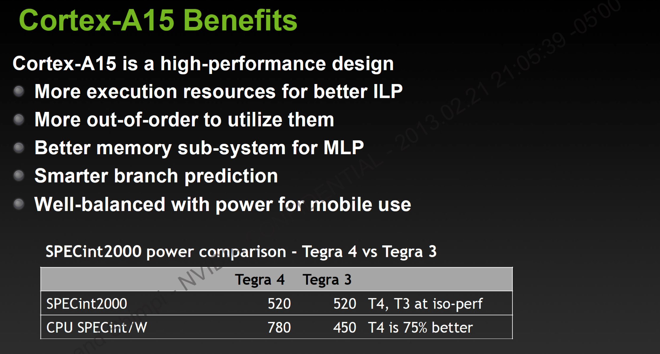
The table above is a bit confusing so let me explain. In the first row NVIDIA is showing that it has configured the Tegra 3 and 4 platforms to deliver the same SPECint_base 2000 performance. SPECint is a well respected CPU benchmark that stresses everything from the CPU core to the memory interface. The int at the end of the name implies that we’re looking at purely single threaded integer performance.
The second row shows us the SPECint per watt of the Tegra 3/4 CPU subsystem, when running at the frequencies required to deliver a SPECint score of 520. By itself this doesn’t tell us a whole lot, but we can use this data to get some actual power numbers.
At the same performance level, Tegra 4 operates at 40% lower power than Tegra 3. The comparison is unfortunately not quite apples to apples as we’re artificially limiting Tegra 4’s peak clock speed, while running Tegra 3 at its highest, most power hungry state. The clocks in question are 1.6GHz for Tegra 3 and 825MHz for Tegra 4. Running at lower clocks allows you to run at a lower voltage, which results in much lower power consumption. In other words, NVIDIA’s comparison is useful but skewed in favor of Tegra 4.
What this data does tell us however is exactly how NVIDIA plans on getting Tegra 4 into a phone: by aggressively limiting frequency. If a Cortex A15 at 825MHz delivers identical performance at a lower power compared to a 40nm Cortex A9 at 1.6GHz, it’s likely possible to deliver a marginal performance boost without breaking the power bank.
That 825MHz mark ends up being an important number, because that’s where the fifth companion Cortex A15 tops out at. I suspect that in a phone configuration NVIDIA might keep everything running on the companion core for as long as possible, which would address my fears about typical power consumption in a phone. Peak power consumption is still going to be a problem I think.


75 Comments
View All Comments
klmccaughey - Sunday, February 24, 2013 - link
Definitely. All good for us too! :)twotwotwo - Sunday, February 24, 2013 - link
> In the PC industry we learned that there’s no real downside to quad-core as long as you can power gate individual cores, and turbo up to higher frequencies when fewer than four cores are active, there’s no real tradeoff other than cost.I'm not completely sure, because there are always other possible uses for die area.
You could do the big/little thing with A7 'companion' cores, like Samsung. You could use even more area for GPU, like Apple. Wiki suggests you could double the L2 cache to 4MB (though more cache would always be eating power, even with only one core turned on).
But in favor of quad-core: software might start using cores a little more effectively w/time--Google and Apple are apparently trying to make WebKit able to do things like HTML parsing and JavaScript garbage collection in the background, and Microsoft's browser team backgrounds JavaScript compilation. And the other uses of space are also only sort-of useful, and cores (like GHz) are handy for marketing. I can't say I know what the right tradeoff for NVidia is, only that there were were other seemingly-interesting options.
guidryp - Sunday, February 24, 2013 - link
"there are always other possible uses for die area"Yes, in the case of Tegra 3, they could certainly have used extra GPU power more than 4 CPU cores. But they seem to have remedied that this time.
twotwotwo - Monday, February 25, 2013 - link
Def possible, and what they disclosed in this presentation would suggest they've handled it.All that's working against them, GPU-wise, is that user expectations increased since last gen, and Mali/PowerVR improved. So now T4i needs to drive 1080p phone screens and T4 needs to drive screens like the Nexus 10's, if they want to be the most bleeding-edge, anyway.
But they did talk about large integer-factor improvements in the GPU, so maybe they haven't merely built the GPU that would've been nice to have last gen, but moved up enough to be great this gen.
sosadsohappy - Sunday, February 24, 2013 - link
Samsung has just said it is doing A15-A7 pairing. Saying out the future plans just to keep the crowd excited is not new. That does not rule out the possibility of Qualcomm or Nvidia going for similar big.LITTLE designs. They are for the next-gen I would think. (Tell me if I am wrong but have anyone sampled big.LITTLE based SoC yet?)And talking about die area, what is impressive about Nvidia is how their chips are always smaller. Quad-core A15 is about 80mm^2 while you can check for the sizes of Qualcomm's or Apple's chips! FWIW Apple's are not in 28nm but still they don't scale equally.
I am excited to see the 60mm^2 (right?) chip (Tegra4i). If it is what they claim, it should have great battery life for a smartphone.
s44 - Monday, February 25, 2013 - link
4+1 is Nvidia's version of big.LITTLE. The 1 low-power A15 is about the same die space as the 4 A7s on the next Exynos...sosadsohappy - Monday, February 25, 2013 - link
Yes. The only difference is that the big.LITTLE will sport different architectures on the big and LITTLE while NV's 4+1 will have the same arch (A15 for both).And personally I think 4+1 is better as of now until we have Atlas and Apollo combination of big.LITTLE because (correct me if I'm wrong) A7 does not have as much of memory parallelism, it is to weak as well...
No matter what, it has been impressive that Nvidia chips have significantly lower die size than the competition's dual-core chips!
Krysto - Monday, February 25, 2013 - link
Too weak? For what? Receiving notifications? We'll see if Tegra 4 is more energy efficient than Samsung's Exynos 5 Octa later this year. Then we might get a better idea whether Nvidia or ARM's implementation is better.And I agree. Nvidia managed to have the same graphics performance + a quad core Cortex A15 CPU in 80mm2 vs Apple with a dual core CPU and same graphics performance in 120 mm2. That's pretty impressive, even if it arrives half a year late.
I still wish Nvidia would actually want to compete at the high-end though, with a 120mm2 chip, and beat Apple. It annoys me that they are still trying to build only "good enough for most people" chips. They should be trying to be the king of mobile graphics. They are freaking Nvidia, and they can't even beat a mobile GPU maker? Come on, Nvidia.
name99 - Monday, February 25, 2013 - link
> In the PC industry we learned that there’s no real downside to quad-core as long as you can power gate individual cores, and turbo up to higher frequencies when fewer than four cores are active, there’s no real tradeoff other than cost.Sony Ericsson recently released a paper claiming this was not true, even apart from the die area issues. In particular they claimed that with current technology, coupling capacitance, ground plane issues, communication (with the L2, including coherence) and suchlike, quad-core imposed something like a 25% reduction in peak MHz possible for two cores, compared to those same two cores isolated rather than on a quad-core die.
Now obviously any company publication is talking up its book, but I imagine they're not going to make a statement that is blatantly false in a technical publication, implying there is some truth to what they say.
Wilco1 - Wednesday, February 27, 2013 - link
Given Tegra 4i achieves 2.3GHz in a quad core with shared L2, way more than Krait which uses per-CPU L2, I think the claim that a shared L2 is clock limiting seems more marketing than substance.