NVIDIA Tegra 4 Architecture Deep Dive, Plus Tegra 4i, Icera i500 & Phoenix Hands On
by Anand Lal Shimpi & Brian Klug on February 24, 2013 3:00 PM ESTThe GPU
Tegra 4 features an evolved GPU core compared to Tegra 3. The architecture retains a fixed division between pixel and vertex shader hardware, making it the only modern mobile GPU architecture not to adopt a unified shader model.
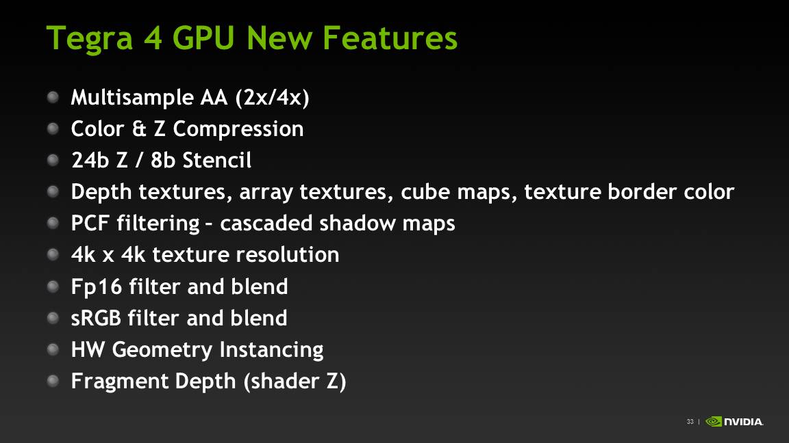

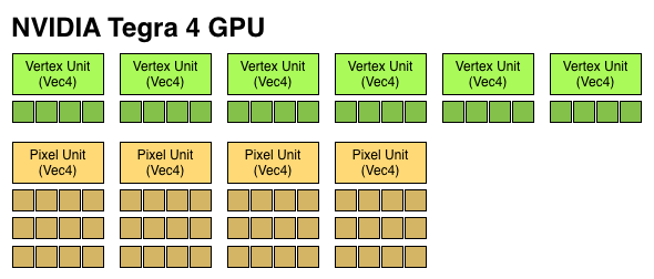
I already described a lot of what makes the Tegra 4 GPU different in our original article on the topic. The diagram below gives you an idea of how the pixel and vertex shader hardware grew over the past 3 generations:
We finally have a competitive GPU architecture from NVIDIA. It’s hardly industry leading in terms of specs, but there’s a good amount of the 80mm^2 die dedicated towards pixel and vertex shading hardware. There's also a new L2 texture cache that helps improve overall bandwidth efficiency.
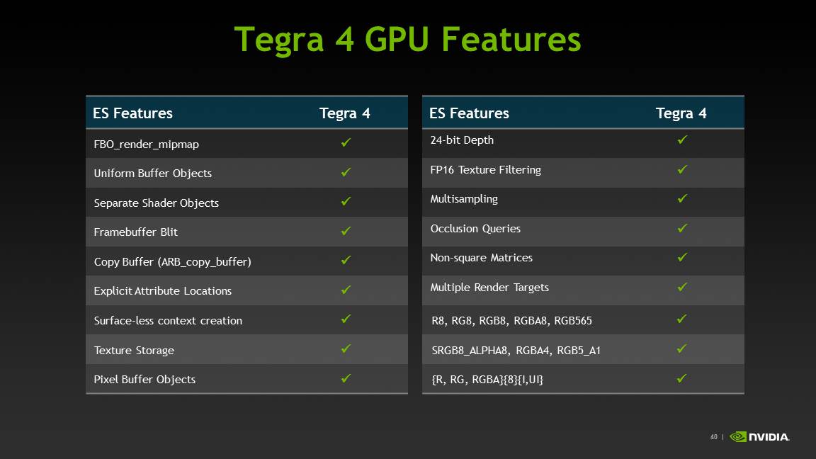
The big omission here is the lack of full OpenGL ES 3.0 support. NVIDIA’s pixel shader hardware remains FP24, while the ES 3.0 spec requires full FP32 support for both pixel and vertex shaders. NVIDIA also lacks ETC and FP texture support, although some features of ES 3.0 are implemented (e.g. Multiple Render Targets).
| Mobile SoC GPU Comparison | |||||||||||||||
| GeForce ULP (2012) | PowerVR SGX 543MP2 | PowerVR SGX 543MP4 | PowerVR SGX 544MP3 | PowerVR SGX 554MP4 | GeForce ULP (2013) | ||||||||||
| Used In | Tegra 3 | A5 | A5X | Exynos 5 Octa | A6X | Tegra 4 | |||||||||
| SIMD Name | core | USSE2 | USSE2 | USSE2 | USSE2 | core | |||||||||
| # of SIMDs | 3 | 8 | 16 | 12 | 32 | 18 | |||||||||
| MADs per SIMD | 4 | 4 | 4 | 4 | 4 | 4 | |||||||||
| Total MADs | 12 | 32 | 64 | 48 | 128 | 72 | |||||||||
| GFLOPS @ Shipping Frequency | 12.4 GFLOPS | 16.0 GFLOPS | 32.0 GFLOPS | 51.1 GFLOPS | 71.6 GFLOPS | 74.8 GFLOPS | |||||||||
For users today, the lack of OpenGL ES 3.0 support likely doesn’t matter - but it’ll matter more in a year or two when game developers start using OpenGL ES 3.0. NVIDIA is fully capable of building an OpenGL ES 3.0 enabled GPU, and I suspect the resistance here boils down to wanting to win performance comparisons today without making die size any larger than it needs to be. Remembering back to the earlier discussion about NVIDIA’s cost position in the market, this decision makes sense from NVIDIA’s stance although it’s not great for the industry as a whole.
Tegra 4i retains the same base GPU architecture as Tegra 4, but dramatically cuts down on hardware. NVIDIA goes from 4 down to 3 vertex units, and moves to two larger pixel shader units (increasing the ratio of compute to texture hardware in the T4i GPU). The max T4i GPU clock drops a bit down to 660MHz, but that still gives it substantially more performance than NVIDIA’s Tegra 3.
Memory Interface
The first three generations of Tegra SoCs had an embarrassingly small amount of memory bandwidth, at least compared to Apple, Samsung and Qualcomm. Admittedly, Samsung and Qualcomm were late adopters of a dual-channel memory interface, but they still got there much quicker than NVIDIA did.
With Tegra 4, complaints about memory bandwidth can finally be thrown out the window. The Tegra 4 SoC features two 32-bit LPDDR3 memory interfaces, bringing it up to par with the competition. The current max data rate supported by Tegra 4’s memory interfaces is 1866MHz, but that may go up in the future.
Tegra 4 won’t ship in a PoP (package-on-package) configuration and will have to be paired with external DRAM. This will limit Tegra 4 to larger devices, but it should still be able to fit in a phone.
Unfortunately, Tegra 4i only has a single channel LPDDR3 memory interface. Tegra 4i on the other hand will be available in PoP as well as discrete configurations. The PoP configuration may top out at LPDDR3-1600, while the discrete version can scale up to 1866MHz and beyond.


75 Comments
View All Comments
Death666Angel - Wednesday, February 27, 2013 - link
Get a life.StormyParis - Sunday, February 24, 2013 - link
I'd go with Anand, anytime. Charlie is a raving bitch.mayankleoboy1 - Sunday, February 24, 2013 - link
Except that this raving bitch has accurately predicted the future course of most companies months before anybody.Avalon - Monday, February 25, 2013 - link
If by accurate you mean he made many predictions for every company and when one of the predictions came true everyone forgot about all the wrong ones. He guesses.Kiste - Monday, February 25, 2013 - link
Confirmation bias ahoy!AmdInside - Monday, February 25, 2013 - link
Are you kidding me? Even congress lies less than Charlie does.jjj - Sunday, February 24, 2013 - link
I wouldn't expect a huge downclock for phones , they do need to limit heat, not going with POP for the RAM helps ,some actual cooling (air gap or metal) could also be used so they will most likely allow 1-2 cores to go pretty high and maybe all 4 for short periods of time (so the usual tricks to get more out of it).R3MF - Sunday, February 24, 2013 - link
re tegra 4 gpu architecture.how did you get through this many words without mentioning OpenCL?
lack of ES 3.0 is only half the problem.
cmikeh2 - Sunday, February 24, 2013 - link
He does reference it when discussing the Chimera ISP:"At the same time, the elephant in the room is OpenCL (and its current absence on Tegra 4) and what direction the industry will take that to leverage GPU compute for some computational photography processing."
guidryp - Sunday, February 24, 2013 - link
The Icera acquisition was a brilliant one. This gives NVidia the complete mobile package. It will be very interesting to see how this works out in practice. NVidia is a fierce competitor, Qualcomm should be worried.