NVIDIA Tegra 4 Architecture Deep Dive, Plus Tegra 4i, Icera i500 & Phoenix Hands On
by Anand Lal Shimpi & Brian Klug on February 24, 2013 3:00 PM ESTThe GPU
Tegra 4 features an evolved GPU core compared to Tegra 3. The architecture retains a fixed division between pixel and vertex shader hardware, making it the only modern mobile GPU architecture not to adopt a unified shader model.
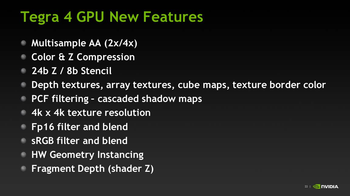

I already described a lot of what makes the Tegra 4 GPU different in our original article on the topic. The diagram below gives you an idea of how the pixel and vertex shader hardware grew over the past 3 generations:
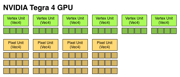
We finally have a competitive GPU architecture from NVIDIA. It’s hardly industry leading in terms of specs, but there’s a good amount of the 80mm^2 die dedicated towards pixel and vertex shading hardware. There's also a new L2 texture cache that helps improve overall bandwidth efficiency.
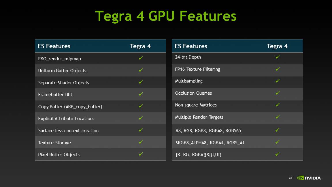
The big omission here is the lack of full OpenGL ES 3.0 support. NVIDIA’s pixel shader hardware remains FP24, while the ES 3.0 spec requires full FP32 support for both pixel and vertex shaders. NVIDIA also lacks ETC and FP texture support, although some features of ES 3.0 are implemented (e.g. Multiple Render Targets).
| Mobile SoC GPU Comparison | |||||||||||||||
| GeForce ULP (2012) | PowerVR SGX 543MP2 | PowerVR SGX 543MP4 | PowerVR SGX 544MP3 | PowerVR SGX 554MP4 | GeForce ULP (2013) | ||||||||||
| Used In | Tegra 3 | A5 | A5X | Exynos 5 Octa | A6X | Tegra 4 | |||||||||
| SIMD Name | core | USSE2 | USSE2 | USSE2 | USSE2 | core | |||||||||
| # of SIMDs | 3 | 8 | 16 | 12 | 32 | 18 | |||||||||
| MADs per SIMD | 4 | 4 | 4 | 4 | 4 | 4 | |||||||||
| Total MADs | 12 | 32 | 64 | 48 | 128 | 72 | |||||||||
| GFLOPS @ Shipping Frequency | 12.4 GFLOPS | 16.0 GFLOPS | 32.0 GFLOPS | 51.1 GFLOPS | 71.6 GFLOPS | 74.8 GFLOPS | |||||||||
For users today, the lack of OpenGL ES 3.0 support likely doesn’t matter - but it’ll matter more in a year or two when game developers start using OpenGL ES 3.0. NVIDIA is fully capable of building an OpenGL ES 3.0 enabled GPU, and I suspect the resistance here boils down to wanting to win performance comparisons today without making die size any larger than it needs to be. Remembering back to the earlier discussion about NVIDIA’s cost position in the market, this decision makes sense from NVIDIA’s stance although it’s not great for the industry as a whole.
Tegra 4i retains the same base GPU architecture as Tegra 4, but dramatically cuts down on hardware. NVIDIA goes from 4 down to 3 vertex units, and moves to two larger pixel shader units (increasing the ratio of compute to texture hardware in the T4i GPU). The max T4i GPU clock drops a bit down to 660MHz, but that still gives it substantially more performance than NVIDIA’s Tegra 3.
Memory Interface
The first three generations of Tegra SoCs had an embarrassingly small amount of memory bandwidth, at least compared to Apple, Samsung and Qualcomm. Admittedly, Samsung and Qualcomm were late adopters of a dual-channel memory interface, but they still got there much quicker than NVIDIA did.
With Tegra 4, complaints about memory bandwidth can finally be thrown out the window. The Tegra 4 SoC features two 32-bit LPDDR3 memory interfaces, bringing it up to par with the competition. The current max data rate supported by Tegra 4’s memory interfaces is 1866MHz, but that may go up in the future.
Tegra 4 won’t ship in a PoP (package-on-package) configuration and will have to be paired with external DRAM. This will limit Tegra 4 to larger devices, but it should still be able to fit in a phone.
Unfortunately, Tegra 4i only has a single channel LPDDR3 memory interface. Tegra 4i on the other hand will be available in PoP as well as discrete configurations. The PoP configuration may top out at LPDDR3-1600, while the discrete version can scale up to 1866MHz and beyond.


75 Comments
View All Comments
darkich - Monday, February 25, 2013 - link
You should know better than to compare different platforms on sunspider.It's more software than hardware dependant benchmark.
Read the jefkibuule's post
danielfranklin - Wednesday, February 27, 2013 - link
With my own testing ive managed to get my Nexus 10 at between 500-600ms on Sunspider. Clocked at roughly 2ghz. It depends more on the browser, the stock android browser is much faster at this than Chrome and doesnt come with the Nexus 10 or Nexus 4.ilihijan - Sunday, March 3, 2013 - link
I just got paid $6784 working on my laptop using these simple steps leaked on this web page. Make up to $85 per hour doing simple tasks that are so easy to do that you won't forgive yourself if you don't check it out! Weekly payments! Here is what I've been doing Epic2.c(om)GiantPandaMan - Sunday, February 24, 2013 - link
Given the vastly different conclusions and what not, I think it would be interesting if Charlie and Anand had a roundtable discussion about the SoC space, both phone and tablet. Has Tegra had a noticeable lack of design wins? Has nVidia overpromised and underdelivered three times in a row? Or is Charlie exaggerating far too much?I'm making no judgement myself, since I really know very little about how phone and tablet manufacturers view the various SoC's.
Have you guys reached out to manufacturers and gotten their takes at all?
s44 - Sunday, February 24, 2013 - link
What, Charlie pushing anti-Nvidia storylines? Who'd have imagined that.lmcd - Sunday, February 24, 2013 - link
I feel like T2 underperformed because the software on it underperformed (see DX2), as Honeycomb was a pretty terrible release.Tegra 3 didn't do poorly at all. It performed phenomenally as a cheap chip (though the high-clocked ones on high-end phones made no sense). 28nm was a must-have for a high-end chip that generation.
Tegra 4 looks about where everyone expected it. No one should have been surprised with any of those units on the performance levels.
lmcd - Sunday, February 24, 2013 - link
DX2 and Honeycomb not being the same subject of course.But 2.3 was equally bad
rahvin - Monday, February 25, 2013 - link
A lot of what Charlie said is easily check-able. Tegra2 had a ton of design wins and almost no actual sales. Tegra3 has done phenomenally, but only in tablets and it's already been replaced in one or two. I think the most prophetic thing he said is the most obvious, unlike every previous generation they didn't announce a single design win for Tegra4. That to me speaks volumes.We'll know in time if it's just the vendetta or if his sources are correct. I've never heard of a chip maker doing a reference design and personally I just don't see that having any effect or why they would even do it. The manufacturers like to differentiate and the reference design takes that away, which again speaks to lack of manufacturer interest. Charlie tends to over exaggerate things but IMO he's been fairly spot on. Even with the highest revenue in their history profit was down almost 25% (which I attribute to the change to paying for wafer instead of good chips).
Again, time will tell.
Kidster3001 - Thursday, February 28, 2013 - link
FFRD is popular for companies that only produce the chips and not any phones themselves. Samsung has no need to do it, Apple either. Who's left? Qualcomm sells (almost) reference designs with their MDP, Intel's first two phones (Lava Xolo and Orange Santa Clara) were basically rebadged reference devices. Now NVidia's doing it. One advantage to having an FFRD is so that the customer can bring it to market faster and cheaper. OEM's like that and it also allows for chip manufacturers to get their stuff into the hands of smaller OEMs who don't have large R&D budgets.All the Tegra chips have had higher power consumption than their peers from other manufacturers. It looks like Tegra4 is no exception. They work well in tablets where it is less important, but poor battery life is a really good reason for OEM's to not make phones based on your chips.
My personal opinion is that A15 (ARMs core) will never be a really good design for a phone. It has really high performance but the power envelope just isn't going to work. Those who design custom cores will come out ahead in the phone battle: Apple, Qualcomm, Intel and perhaps even NVidia if they move away from ARM IP with their Denver design.
TheJian - Monday, February 25, 2013 - link
Charlie has hated NV forever. He did the same crap at theINQ for years. At least he named his site accurately...ROFL. Actually I enjoy reading (used to) some of his stuff, but when he speaks about NV I'd say his site should have been named usuallynotaccurate.comNow he's actually charging for semiaccurate articles...LOL
Seriously? If it was that important I'd rather pay for something like MPR. Charlie is usually good for a laugh and that's about it regarding NV.
Though I've written some stuff about this site's bias recently (my titan article posts and the 660ti article comments), I don't think anandtech and semiaccurate sit at the same table. Anandtech isn't making stuff up, they're just leaving out 3/4 of the story IMHO (regarding my comments on the 14games etc that should be in the game suite & the two that shouldn't). Charlie just throws darts at a board for a large portion of his articles. IF you keep his articles (I did for a long time) and go back over them he's only right about 50%. Either he's getting WMD like UK info (ala bush and iraq, though I think they just moved them to syria...LOL we gave them ages to move them) or he just makes it up himself ("my deep mole in x company said blah blah"). There's no proof until ages later when most forget what he even said, right or wrong. Note there is NO COMMENT section on the site now. They're all blocked :) Ubergizmo called his site "half accurate". My data of old articles used to say the same :) I expect more than flipping a coin results in reporting. He gets credit for things like breaking the news on the bapco fiasco, but I'd say Van Smith gets credit for exposing not only that Intel OWNED the land they had their building on (they paid rent to Intel), Intel OWNED their domain name, and even had a hand in WRITING the code as Intel software engineers were on hand next door. Van covered it all YEARS before Charlie. Look up Van smith and vanshardware, a lot of that crap and the biased intel reporting forced Van to leave and probably dropped the price of Toms site to 1/4 of it's value when tom dumped it. He was worth MORE than anandtech before that stuff. Not sure of the value today, I'm talking back then.
Biased reporting gets you killed if the right people keep pointing it out with DATA backing it. IF Tom's hadn't gone down that Intel love-in route he probably could have sold for much more. There's a reason Otellini said in 2006 that toms was his favorite tech site ;) Then in turn dumped the site as it's credibility tanked. Bapco was, and still is a sham. AMD/NV/VIA all left the consortium for a reason. I don't put much stock in anything from them (futuremark either). Tom's treatment of Van (even removed his bylines on stories) was downright disgusting. I stopped reading toms for about 5 years due to that crap in ~2001. He replaced every article the guy wrote with "THG staff". Total BS. Charlie does the same with NV hate as toms with Intel love. This crap costs credibility.
Anandtech is coming close to the same thing on NV gpu's; Ryan's AMD love anyway, I'll bang away until he stops :) Funny how they never attack the data I provide here. I link to them at toms forums too, eventually that will begin to hurt as people look at the evidence and draw their own conclusions about his articles and in turn this site's credibility. If he continues on the next reviews (700's and 8000's) I'll get on a lot more forums linking the comments after the data dismantling (polite critique of course Ryan :)).
The "Jian" is a double edged sword Ryan ;) Thin, light and very maneuverable...LOL
https://en.wikipedia.org/wiki/Jian
In Chinese folklore, it is known as "The Gentleman of Weapons"
I'm not hostile Ryan ;) Wikipedia says so. :)
Google this: thejian anandtech
Data piles up don't it? I save all my posts (before posting) anyway, but google does too.