NVIDIA Tegra 4 Architecture Deep Dive, Plus Tegra 4i, Icera i500 & Phoenix Hands On
by Anand Lal Shimpi & Brian Klug on February 24, 2013 3:00 PM ESTIt basically goes without saying, but Tegra 4i, formerly Grey, is primarily a story about the modem. About halfway through 2011, NVIDIA acquired Icera, a player in the handset cellular baseband market who had managed to fit a software-defined radio into the power budget for a mobile device. NVIDIA clearly recognized the importance of being able to deliver an SoC with an integrated modem, and after the Icera acquisition, and later Grey’s appearance on the roadmap, it just became a matter of when that would happen. NVIDIA executed pretty quickly, it turns out, and the fruits of that work manifest themselves in two products — Icera’s standalone i500 and Tegra 4i which contains the same i500 IP block, minus USB interfaces and a different memory subsystem.

Icera was an interesting player in the baseband space because their architecture was that of a software defined radio on the digital baseband side. The reality is that nobody is either fully software defined or burned out to ASIC (hardware), but rather somewhere inbetween. For example, Qualcomm is a combination of software and hardware, though it’s never been entirely clear what functional blocks are ASIC and which other blocks are software, though I’ve been told this is often a matter of whatever is most advantageous for power and what gets re-used most. That said, Icera’s implementation is the furthest towards being pure software defined of anyone, with the entire digital baseband being just one big platform to run their own software atop. There’s an external transceiver which does downconversion, but after that it’s pure software. The question has always been how Icera could afford to build a power competitive platform with an entirely software designed stack, and the clue lies in their choice of 28 HPM instead of LP or HPL silicon for i500 and 4i. Icera designs to a high performance process, then turns off blocks when they’re not in use, rather than make a larger SoC that’s lower leakage. The result is that NVIDIA claims a 40% smaller die for i500 than MDM9x15.
Icera has maintained the same software platform across its modem portfolio, each time taking advantage of increased processing performance afforded by faster silicon to include more air interfaces and capabilities. The result is an interesting advantage when it comes to operator certification — they can make a compelling case for each new version being close to the previous one, since they run the same PHY and protocol stack entirely in software.

In the case of i500, it runs the exact same multimode modem software as the i4xx series, just with increased DXP support for 15 and 20 MHz channel bandwidths on LTE.
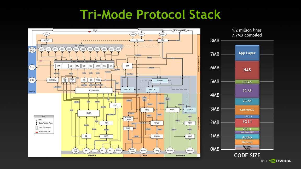
The entire stack ends up being 1.2 million lines of C and DXP code, with a total size of 7.7 MB compiled. NVIDIA gave a great breakdown of the protocol stack as well.
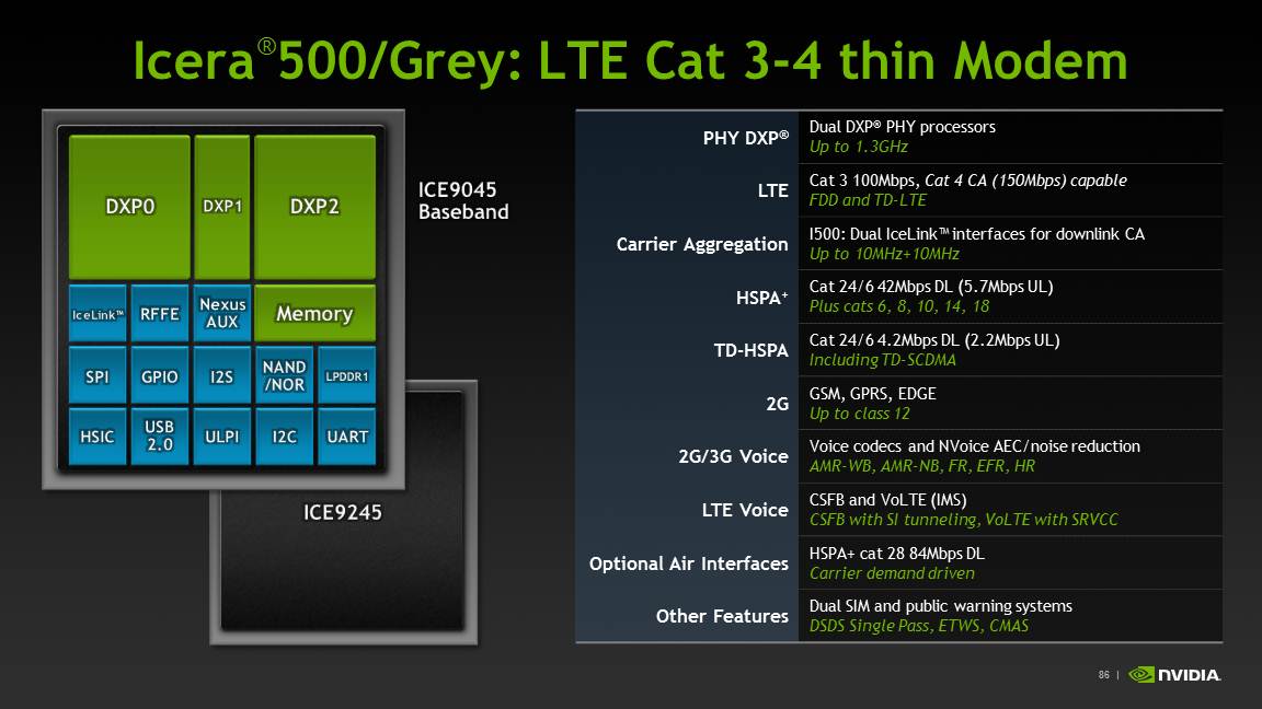
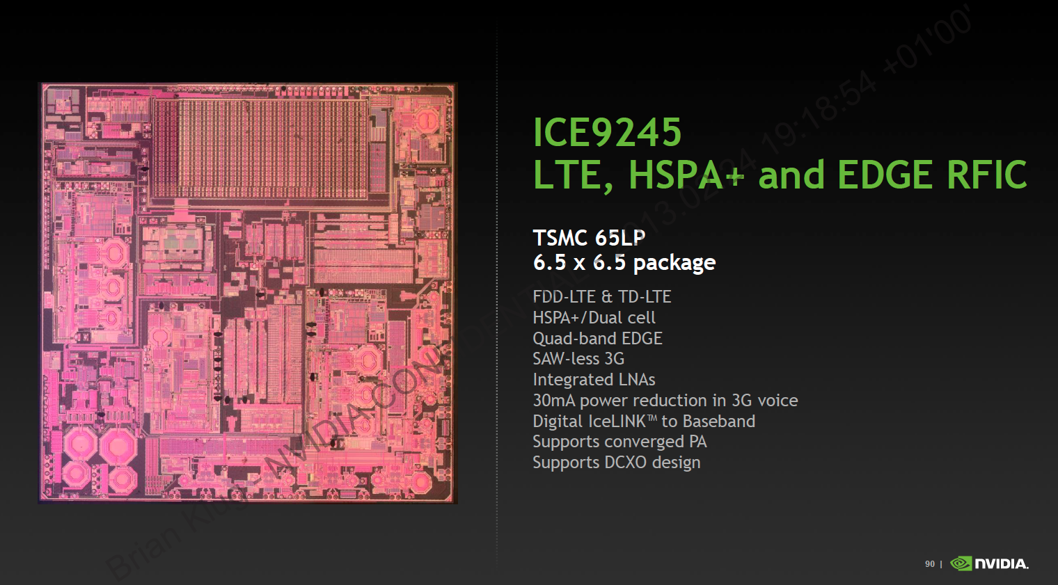
The real name for Icera i500 is ICE9045, and it is paired with a ICE9245 transceiver. ICE9045 is built on 28nm HPM as I mentioned before, and ICE9245 remains 65nm TSMC LP CMOS process which is RF friendly. ICE9045 supports basically all the 3GPP air interfaces, as mentioned in the earlier announcement piece. There’s up to Category 3 LTE on the baseband at launch, with Category 4 in the future. For WCDMA, up to Category 24 (42 Mbps) (dual carrier with 64QAM), and interestingly enough the same Category 18 16 QAM with 2x2 MIMO (28 Mbps) as earlier implemented in Icera 450, and an optional future upgrade to Category 28 64 QAM with 2x2 MIMO (84 Mbps). Of course there’s also TD-SCDMA, GSM/EDGE, full support for voice including AMR-WB and VoLTE/IMS. In addition to 2x2 MIMO the ICE9045 can also do 4x4 MIMO on LTE with a second ICE9245 transceiver.

NVIDIA broke down the ICE9045 functionally, which consists of two large DXP units and one smaller DXP unit which runs the rest of the software and management stack. The two larger DXP units run at up to 1.3 GHz. The Icera instruction set consists of two different fundamental sets. Icera refers to these as the “C” and “D” side, with C being rather obvious. The C side is unsurprisingly a C-complier targeted version of the 3GPP protocol stack, and manages the higher level functions of the modem above physical interface, and is a scalar machine. In the block diagram, the C side runs on DXP1, the D side runs on the larger beefier DXP0 and DXP2 machines.
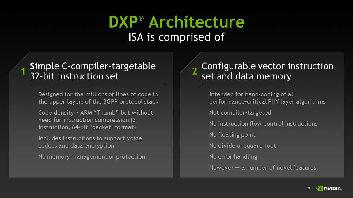
The D side is a proprietary assembly language vector instruction set that runs the physical layer of the modem, this is a combination of specific libraries that really make up the magic and give the Icera platform its reconfigurability. NVIDIA gave an excellent breakdown of the data paths inside both sides. It turns out that in an LTE configuration one core does all the inverse FFTs and MIMO matrix math, the second core does rate matching and decoding. The ultimate goal is to have each of the cores processing around the same equal workload, and since it’s software these tasks can be shuffled in-between to get the i500 running each core at the lowest possible frequency and voltage. Each of the cores can also be individually power collapsed.
On the transceiver side we have ICE9245 which is again TSMC 65nm LP CMOS. This talks over a digital interface to the baseband, and increases the number of primary RX ports from 6 to 8. All filtering and channelization is onboard the ISP. The goal is to keep all the A2D and D2A on the transceiver and away from the baseband. NVIDIA hasn’t quite given me the frequency breakdown for their low band, high band, and super high band, but you can figure it out just by looking. There’s also diversity ports for the same set of bands. All these ports are created equal and can handle 20 MHz LTE, in addition to inter-band and intra-band CA.
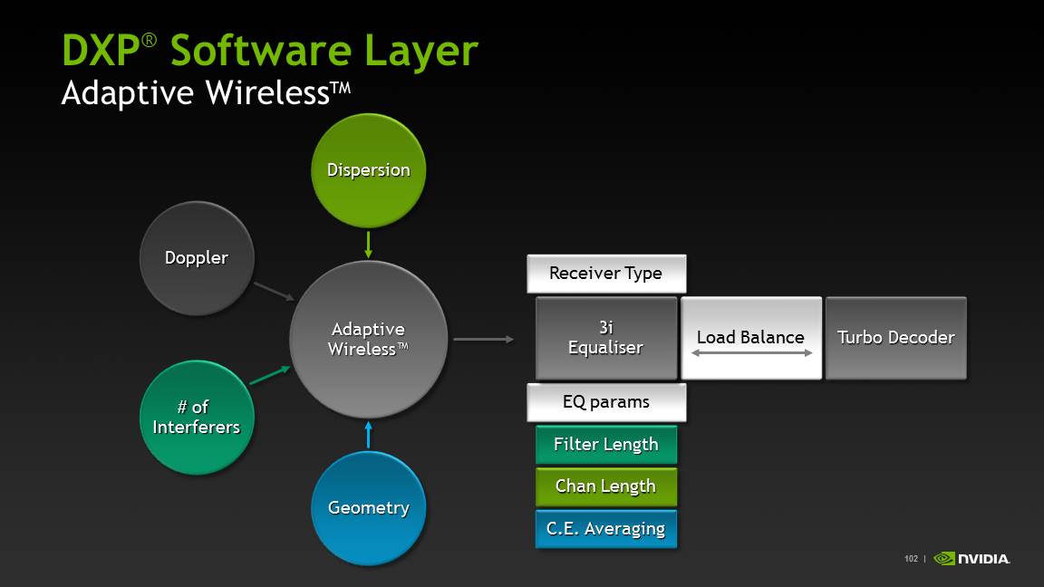
The big question is how well Icera’s i500 will stack up against the MDM9x15s and MDM9x25s of the world. Icera believes its ability to switch between four fundamentally different receiver types on the fly and dedicate processing to different functions based on the cellular geometry at the moment offers it an advantage in the long run.
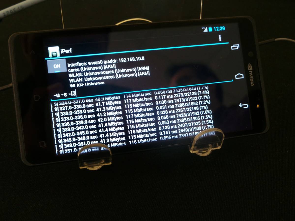
NVIDIA demonstrated a Phoenix with Tegra 4i cabled up to a base station emulator doing full Category 3 LTE at 100 Mbps nice and steady. I asked whether they could go any higher to demonstrate the headroom in the current i500 architecture for upgrading to Category 4 and was shown just short of 120 Mbps on the two week old Tegra 4i silicon.


75 Comments
View All Comments
tipoo - Sunday, February 24, 2013 - link
Under 500 in Sunspider, about twice as fast as anything else ARM. But then again, it's a few months newer than that, and actually still not shipping. And as usual with Nvidia they're early to each party (first to dual core, first to quad core), but not always the best performing. We'll see if other Cortex A15 designs beat it.I'd love to see four of those cores paired with SGXs upcoming 600/Rogue series.
jeffkibuule - Sunday, February 24, 2013 - link
SunSpider is so software sensitive that a Tegra 3 @ 1.2 Ghz on Windows RT beats a Snapdraon S4 Pro @ 1.5Ghz on Nexus 4 using Chrome. It's a terrible benchmark because its so dependent on underlying kernel optimizations in the Android phone market.tipoo - Sunday, February 24, 2013 - link
True, other benchmarks are similarly impressive though.karasaj - Sunday, February 24, 2013 - link
Psh it has nothing on my desktop! 125ms on sunspider... Nvidia so behind.Anyways, still looks impressive. I really want to see some Krait 600/800 benchmarks.
tipoo - Sunday, February 24, 2013 - link
The fact that they're getting well below an order of magnitude slower than desktops is impressive in itself too. Even with iPad 2 level performance I still was reluctant to do most of my web browsing on a tablet for the performance. Maybe with Tegra 4 and beyond hardware speed that will change.Mumrik - Sunday, February 24, 2013 - link
As someone with heavily tabbed browsing habits, I don't think I'll ever make that jump (and I own a tablet).tipoo - Sunday, February 24, 2013 - link
Also true, that's my other thing. I like to open a bunch of background tabs and have them ready as I go through each one. Right now, tablets don't do background loading, as far as I know, and if they did they wouldn't be powerful enough to keep the main tab smooth while doing it.Tarwin - Monday, February 25, 2013 - link
Tablets DO do background loading, as long as they're android. The only performance I've seen is from lack of RAM on my phone and lack of bandwidth on the phone and tablet but those things affect any computer as well. One observation to ne made, they do load in the background but things like audio and video playback will pause if you switch to another tab.von Krupp - Monday, February 25, 2013 - link
Even Windows Phone 7.5 and 8 do background loading. I haven't used it, but I'd wager that RT does as well, if even the gimpy mobile OS can.tuxRoller - Sunday, February 24, 2013 - link
As someone who had, until recently, over 40 tabs open on my chrome browser (Nexus 4), the critical problem has been memory. With enough memory, and good enough task management, these problems tend to go away.Of course, maybe you are than 0.00001% who has hundreds or thousands of tabs open in which case I pity any computer you are likely to own.