Samsung Details Exynos 5 Octa Architecture & Power at ISSCC '13
by Anand Lal Shimpi on February 20, 2013 12:42 PM EST- Posted in
- SoCs
- Samsung
- Arm
- Cortex A15
- Cortex A7
- exynos 5 octa
At CES this year Samsung introduced the oddly named Exynos 5 Octa SoC, one of the first Cortex A15 SoCs to implement ARM's big.LITTLE architecture. Widely expected to be used in the upcoming Galaxy S 4, the Exynos 5 Octa integrates 4 ARM Cortex A7 cores and 4 ARM Cortex A15 cores on a single 28nm LP HK+MG die made at Samsung's own foundry. As we later discovered, the Exynos 5 Octa abandons ARM's Mali GPU for Imagination's PowerVR SGX 544MP3, which should give it GPU performance somewhere between an iPad 3 and iPad 4.
The quad-core A7 can run at between 200MHz and 1.2GHz, while the quad-core A15 can run at a range of 200MHz to 1.8GHz. Each core can be power gated independently. The idea is that most workloads will run on the quad-core A7, with your OS hot plugging additional cores as performance demands increase. After a certain point however, the platform will power down the A7s and start switching over to the A15s. Both SoCs implement the same revision of the ARM ISA, enabling seamless switching between cores. While it's possible for you to use both in parallel, initial software implementations will likely just allow you to run on the A7 or A15 clusters and switch based on performance requirements.
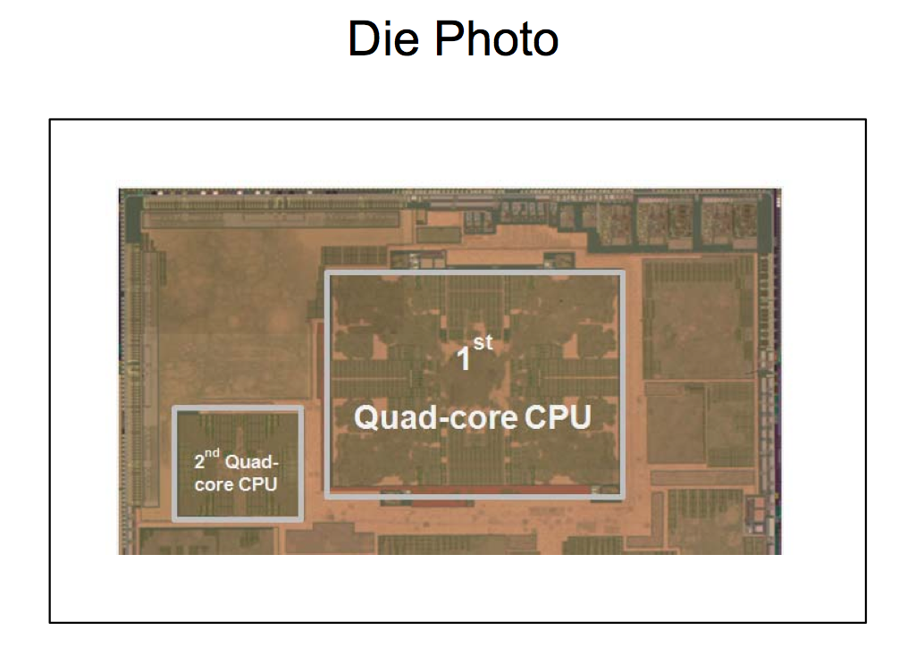
What's most interesting about Samsung's ISSCC presentation is we finally have some hard power and area data comparing the Cortex A15 to the Cortex A7. The table above puts it into numbers. The quad-core A15 cluster occupies 5x the area of the quad-core A7 cluster, and consumes nearly 6x the power in the worst case scenario. The area difference is artificially inflated by the fact that the A15 cluster has an L2 cache that's 4x the size of the A7 cluster, but looking at the die photo below you can get a good feel for just how much bigger the A15 cores are themselves:
In its ISSCC presentation, Samsung stressed the value of its custom libraries, timing tweaks and process technology selection in bringing the Exynos 5 Octa to market. Samsung is definitely marching towards being a real player in the SoC space and not just another ARM licensee.
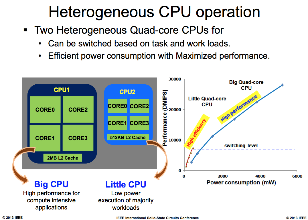
The chart below is one of the most interesting, it shows the relationship between small integer code performance and power consumption on the Cortex A7 and A15 clusters. Before switching from the little CPU to the big one, power consumption is actually quite reasonable - south of 1W and what you'd expect for a smartphone or low power tablet SoC. At the lower end of the performance curve for the big CPU things aren't too bad either, but once you start ramping up clock speed and core count power scales linearly. Based on this graph, it looks like it takes more than 3x the power to get 2x the performance of the A7 cluster using the Cortex A15s.


52 Comments
View All Comments
alexvoda - Wednesday, February 20, 2013 - link
Is it me or is the layout of that chip really inefficient?I'm not really knowledgeable in chip design but I think the orange brown area around the CPU may possibly be wasted surface.
At least compared to these:
http://www.anandtech.com/show/6323/apple-a6-die-re...
http://www.anandtech.com/show/6472/ipad-4-late-201...
http://www.anandtech.com/show/5831/amd-trinity-rev...
There doesn't seam to be a lot of space left for the GPU.
And since this will probably come in 1080p or higher devices the GPU matters
Death666Angel - Wednesday, February 20, 2013 - link
It's just you. :PThe stuff you linked to has the exact same "orange brown area". And that probably isn't wasted surface.
UpSpin - Wednesday, February 20, 2013 - link
I don't think the die photo shows the whole die, only the upper half maybe.I'm also no chip designer, but maybe the orange brown area gets used for wires to connect the different parts.
The top left part looks odd, not orange brown, not structured, but near the RAM interfaces. Maybe they blurred that part because it contains their 'secret CPU switching' part?
alexvoda - Thursday, February 21, 2013 - link
I see.Yup, the photo only shows half of the die, Really made it more confusing.
I didn't mean wasted and in empty and does nothing but more as in no active component. And if that was the entire die the percentage occupied by the orange brown space would have been huge. Since this is probably just half of the die it matters a lot less.
alex3run - Thursday, February 21, 2013 - link
I think Samsung would unveil more details about this SoC later.Shadowmaster625 - Wednesday, February 20, 2013 - link
I was saying years ago how intel needed to take an atom and stick it on the same die as an i-series chip. And essentially do with them exactly what is described in this article. But of course, they didnt do it, and as a result they lost billions in potential mobile chip sales to companies like apple. Haswell looks kind of like an improvement, but you can tell they're still not doing what needs to be done.90% of the time, a tablet/ultrabook only needs the cpu power of one single atom core. This is the basic fact that has been ignored by intel (and AMD) for more than a decade now. But samsung understands this.
djgandy - Thursday, February 21, 2013 - link
The problem with laptops was not the CPU, it was all the other cheap components that sucked power. Laptop screens are terrible and good value ones still use mechanical hard drives!UpSpin - Thursday, February 21, 2013 - link
No!Extra devices get shut down if not used.
Laptop screens are/were terrible, but this means they are low resolution TN panels. But TN panels have better transmittance than IPS. Low resolution displays have better transmittance than high resolution. I hope you're able to follow, but this means, yes, they are more efficient and don't require such a bright backlight.
The power consumption of a HDD is, in idle, higher than the one of a SSD. But therefore you get more space. And in general, the impact is small compared to the CPU and GPU power consumption.
I'm sorry, your logic is flawed.
Btw: This is an article about the power consumption of a SoC, and only the SoC! Why do you compare it with the power consumption of a whole system? This SoC consumes less power than an Intel CPU/GPU/chipset combo. That's what matters. Nothing else! So don't compare apples with oranges.
shadowmaster is right, your post nonsene.
mayankleoboy1 - Thursday, February 21, 2013 - link
smart move to abandon Mali arch. It was slow compared to the PowerVR GPU's.But is it enough to win benchmarks against iPhone6 and iPad5 ?
And Adreno 320 is a wimp by comparison.
alex3run - Thursday, February 21, 2013 - link
Mali T604 is the same level as PowerVR 554 @280 MHz. And PowerVR 544MP3 is slower than both of those GPUs. So it would be very strange to see it inside Exynos Octa. More likely there will be Mali T658/678MP4 which is twice as fast as anything on the market today.