NVIDIA's GeForce GTX Titan, Part 1: Titan For Gaming, Titan For Compute
by Ryan Smith on February 19, 2013 9:01 AM ESTThe launch of the Kepler family of GPUs in March of 2012 was something of a departure from the normal for NVIDIA. Over the years NVIDIA has come to be known among other things for their big and powerful GPUs. NVIDIA had always produced a large 500mm2+ GPU to serve both as a flagship GPU for their consumer lines and the fundamental GPU for their Quadro and Tesla lines, and have always launched with that big GPU first.
So when the Kepler family launched first with the GK104 and GK107 GPUs – powering the GeForce GTX 680 and GeForce GT 640M respectively – it was unusual to say the least. In place of “Big Kepler”, we got a lean GPU that was built around graphics first and foremost, focusing on efficiency and in the process forgoing a lot of the compute performance NVIDIA had come to be known for in the past generation. The end result of this efficiency paid off nicely for NVIDIA, with GTX 680 handily surpassing AMD’s Radeon HD 7970 at the time of its launch in both raw performance and in power efficiency.
Big Kepler was not forgotten however. First introduced at GTC 2012, GK110 as it would come to be known would be NVIDIA’s traditional big, powerful GPU for the Kepler family. Building upon NVIDIA’s work with GK104 while at the same time following in the footsteps of NVIDIA’s compute-heavy GF100 GPU, GK110 would be NVIDIA’s magnum opus for the Kepler family.
Taped out later than the rest of the Kepler family, GK110 has taken a slightly different route to get to market. Rather than launching in a consumer product first, GK110 was first launched as the heart of NVIDIA’s Tesla K20 family of GPUs, the new cornerstone of NVIDIA’s rapidly growing GPU compute business.
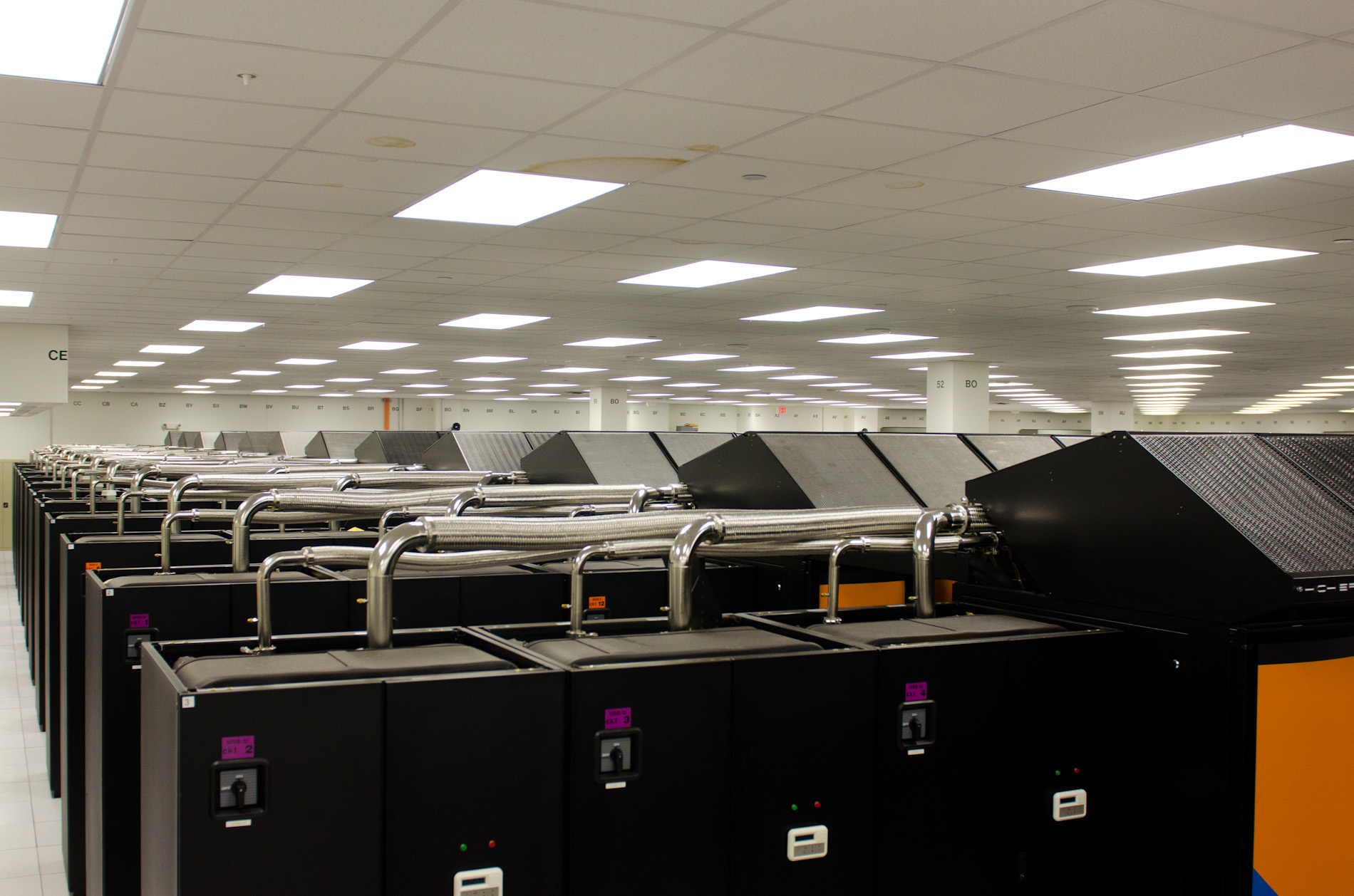
Oak Ridge National Laboratory's Titan Supercomputer
Or perhaps as it’s better known, the GPU at the heart of the world’s fastest supercomputer, Oak Ridge National Laboratory’s Titan supercomputer.
The Titan supercomputer was a major win for NVIDIA, and likely the breakthrough they’ve been looking for. A fledging business merely two generations prior, NVIDIA and their Tesla family have quickly shot up in prestige and size, much to the delight of NVIDIA. Their GPU computing business is still relatively small – consumer GPUs dwarf it and will continue to do so for the foreseeable future – but it’s now a proven business for NVIDIA. More to the point however, winning contracts like Titan are a major source of press and goodwill for the company, and goodwill the company intends to capitalize on.
With the launch of the Titan supercomputer and the Tesla K20 family now behind them, NVIDIA is now ready to focus their attention back on the consumer market. Ready to bring their big and powerful GK110 GPU to the consumer market, in typical NVIDIA fashion they intend to make a spectacle of it. In NVIDIA’s mind there’s only one name suitable for the first consumer card born of the same GPU as their greatest computing project: GeForce GTX Titan.
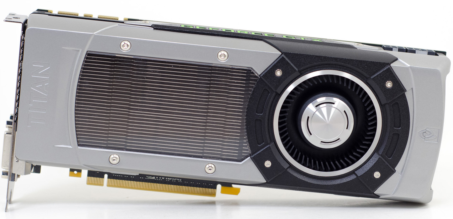
GeForce GTX Titan: By The Numbers
At the time of the GK110 launch at GTC, we didn’t know if and when GK110 would ever make it down to consumer hands. From a practical perspective GTX 680 was still clearly in the lead over AMD’s Radeon HD 7970. Meanwhile the Titan supercomputer was a major contract for NVIDIA, and something they needed to prioritize. 18,688 551mm2 GPUs for a single customer is a very large order, and at the same time orders for Tesla K20 cards were continuing to pour in each and every day after GTC. In the end, yes, GK110 would come to the consumer market. But not until months later, after NVIDIA had the chance to start filling Tesla orders. And today is that day.
Much like the launch of the GTX 690 before it, NVIDIA intends to stretch this launch out a bit to maximize the amount of press they get. Today we can tell you all about Titan – its specs, its construction, and its features – but not about its measured performance. For that you will have to come back on Thursday, when we can give you our benchmarks and performance analysis.
| GTX Titan | GTX 690 | GTX 680 | GTX 580 | |
| Stream Processors | 2688 | 2 x 1536 | 1536 | 512 |
| Texture Units | 224 | 2 x 128 | 128 | 64 |
| ROPs | 48 | 2 x 32 | 32 | 48 |
| Core Clock | 837MHz | 915MHz | 1006MHz | 772MHz |
| Shader Clock | N/A | N/A | N/A | 1544MHz |
| Boost Clock | 876Mhz | 1019MHz | 1058MHz | N/A |
| Memory Clock | 6.008GHz GDDR5 | 6.008GHz GDDR5 | 6.008GHz GDDR5 | 4.008GHz GDDR5 |
| Memory Bus Width | 384-bit | 2 x 256-bit | 256-bit | 384-bit |
| VRAM | 6 | 2 x 2GB | 2GB | 1.5GB |
| FP64 | 1/3 FP32 | 1/24 FP32 | 1/24 FP32 | 1/8 FP32 |
| TDP | 250W | 300W | 195W | 244W |
| Transistor Count | 7.1B | 2 x 3.5B | 3.5B | 3B |
| Manufacturing Process | TSMC 28nm | TSMC 28nm | TSMC 28nm | TSMC 40nm |
| Launch Price | $999 | $999 | $499 | $499 |
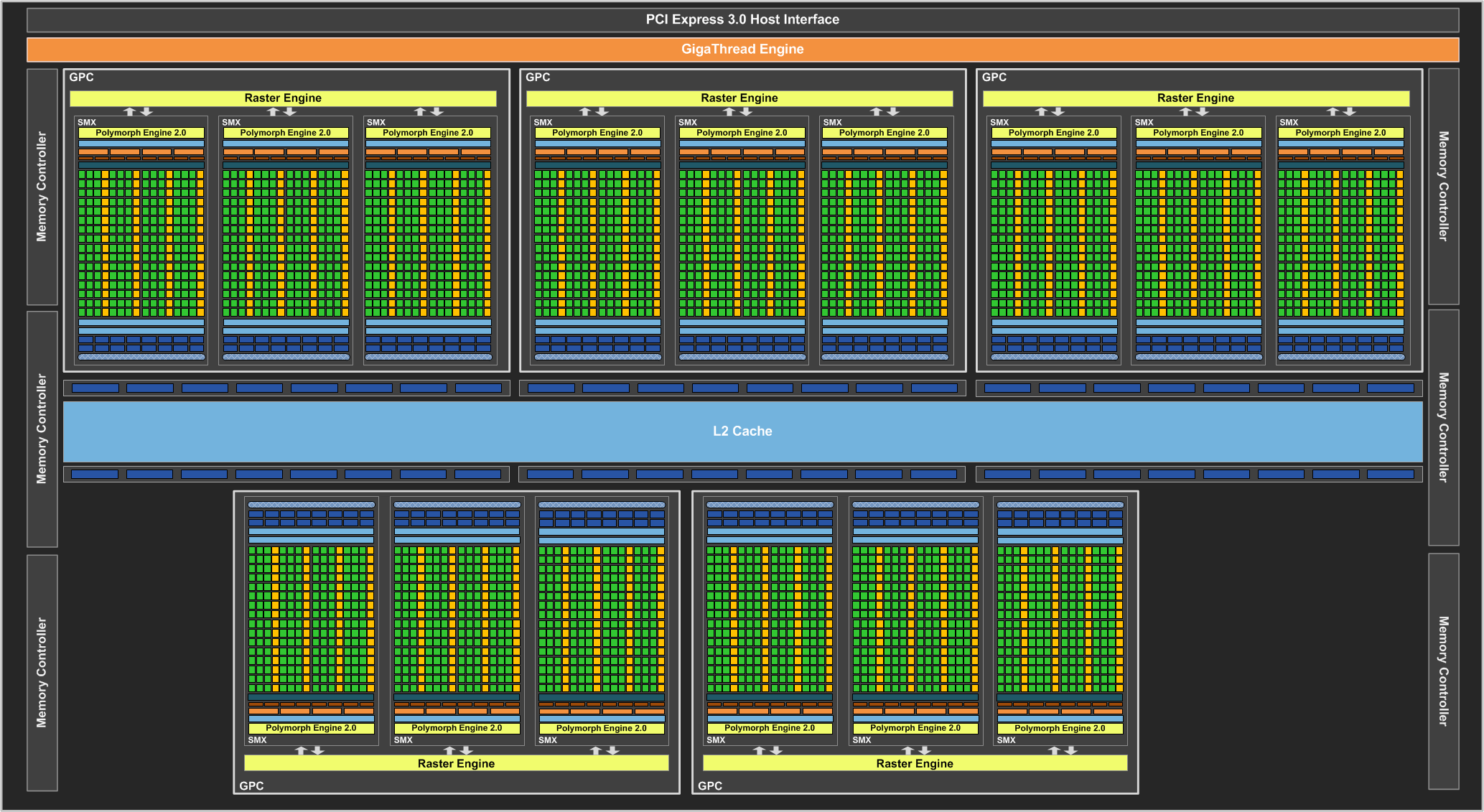
Diving right into things then, at the heart of the GeForce GTX Titan we have the GK110 GPU. By virtue of this being the 2nd product to be launched based off the GK110 GPU, there are no great mysteries here about GK110’s capabilities. We’ve covered GK110 in depth from a compute perspective, so many of these numbers should be familiar with our long-time readers.
GK110 is composed of 15 of NVIDIA’s SMXes, each of which in turn is composed of a number of functional units. Every GK110 packs 192 FP32 CUDA cores, 64 FP64 CUDA cores, 64KB of L1 cache, 65K 32bit registers, and 16 texture units. These SMXes are in turn paired with GK110’s 6 ROP partitions, each one composed of 8 ROPs, 256KB of L2 cache, and connected to a 64bit memory controller. Altogether GK110 is a massive chip, coming in at 7.1 billion transistors, occupying 551mm2 on TSMC’s 28nm process.
For Titan NVIDIA will be using a partially disabled GK110 GPU. Titan will have all 6 ROP partitions and the full 384bit memory bus enabled, but only 14 of the 15 SMXes will be enabled. In terms of functional units this gives Titan a final count of 2688 FP 32 CUDA cores, 896 FP64 CUDA cores, 224 texture units, and 48 ROPs. This makes Titan virtually identical to NVIDIA’s most powerful Tesla, K20X, which ships with the same configuration. NVIDIA does not currently ship any products with all 15 SMXes enabled, and though NVIDIA will never really explain why this is – yield, power, or otherwise – if nothing else it leaves them an obvious outlet for growth if they need to further improve Titan’s performance, by enabling that 15th SMX.
Of course functional units are only half the story, so let’s talk about clockspeeds. As a rule of thumb bigger GPUs don’t clock as high as smaller GPUs, and Titan will be adhering to this rule. Whereas GTX 680 shipped with a base clock of 1006MHz, Titan ships at a more modest 837MHz, making up for any clockspeed disadvantage with the brute force behind having so many functional units. Like GTX 680 (and unlike Tesla), boost clocks are once more present, with Titan’s official boost clock coming in at 876MHz, while the maximum boost clock can potentially be much higher.
On the memory side of things, Titan ships with a full 6GB of GDDR5. As a luxury card NVIDIA went for broke here and simply equipped the card with as much RAM as is technically possible, rather than stopping at 3GB. You wouldn’t know that from looking at their memory clocks though; even with 24 GDDR5 memory chips, NVIDIA is shipping Titan at the same 6GHz effective memory clock as the rest of the high-end GeForce 600 series cards, giving the card 288GB/sec of memory bandwidth.
To put all of this in perspective, on paper (and at base clocks), GTX 680 can offer just shy of 3.1 TFLOPS of FP32 performance, 128GTexels/second texturing throughput, and 32GPixels/second rendering throughput, driven by 192GB/sec of memory bandwidth. Titan on the other hand can offer 4.5 TFLOPS of FP32 performance, 187GTexels/second texturing throughput, 40GPixels/second rendering throughput, and is driven by a 288GB/sec memory bus. This gives Titan 46% more shading/compute and texturing performance, 25% more pixel throughput, and a full 50% more memory bandwidth than GTX 680. Simply put, thanks to GK110 Titan is a far more powerful GPU than what GK104 could accomplish.
Of course with great power comes great power bills, to which Titan is no exception. In GTX 680’s drive for efficiency NVIDIA got GTX 680 down to a TDP of 195W with a power target of 170W, a remarkable position given both the competition and NVIDIA’s prior generation products. Titan on the other hand will have a flat 250W power target – in line with prior generation big NVIDIA GPUs – staking out its own spot on the price/power hierarchy, some 28%-47% higher in power consumption than GTX 680. These values are almost identical to the upper and lower theoretical performance gaps between Titan and GTX 680, so performance is growing in-line with power consumption, but only just. From a practical perspective Titan achieves a similar level of efficiency as GTX 680, but as a full compute chip it’s unquestionably not as lean. There’s a lot of compute baggage present that GK104 didn’t have to deal with.


157 Comments
View All Comments
bigboxes - Tuesday, February 19, 2013 - link
This is Wreckage we're talking about. He's trolling. Nothing to see here. Move along.chizow - Tuesday, February 19, 2013 - link
I agree with his title, that AMD is at fault at the start of all of this, but not necessarily with the rest of his reasonings. Judging from your last paragraph, you probably agree to some degree as well.This all started with AMD's pricing of the 7970, plain and simple. $550 for a card that didn't come anywhere close to justifying the price against the last-gen GTX 580, a good card but completely underwhelming in that flagship slot.
The 7970 pricing allowed Nvidia to:
1) price their mid-range ASIC, GK104, at flagship SKU position
2) undercut AMD to boot, making them look like saints at the time and
3) delay the launch of their true flagship SKU, GK100/110 nearly a full year
4) Jack up the prices of the GK110 as an ultra-premium part.
I saw #4 occurring well over a year ago, which was my biggest concern over the whole 7970 pricing and GK104 product placement fiasco, but I had no idea Nvidia would be so usurous as to charge $1k for it. I was expecting $750-800....$1k....Nvidia can go whistle.
But yes, long story short, Nvidia's greed got us here, but AMD definitely started it all with the 7970 pricing. None of this happens if AMD prices the 7970 in-line with their previous high-end in the $380-$420 range.
TheJian - Wednesday, February 20, 2013 - link
You realize you're dogging amd for pricing when they lost 1.18B for the year correct? Seriously you guys, how are you all not understanding they don't charge ENOUGH for anything they sell? They had to lay of 30% of the workforce, because they don't make any money on your ridiculous pricing. Your idea of pricing is KILLING AMD. It wasn't enough they laid of 30%, lost their fabs, etc...You want AMD to keep losing money by pricing this crap below what they need to survive? This is the same reason they lost the cpu war. They charged less for their chips for the whole 3yrs they were beating Intel's P4/presHOT etc to death in benchmarks...NV isn't charging too much, AMD is charging too LITTLE.AMD has lost 3-4B over the last 10yrs. This means ONE thing. They are not charging you enough to stay in business.
This is not complicated. I'm not asking you guys to do calculus here or something. If I run up X bills to make product Y, and after selling Y can't pay X I need to charge more than I am now or go bankrupt.
Nvidia is greedy because they aren't going to go out of business? Without Intel's money they are making 1/2 what they did 5yrs ago. I think they should charge more, but this is NOT gouging or they'd be making some GOUGING like profits correct? I guess none of you will be happy until they are both out of business...LOL
chizow - Wednesday, February 20, 2013 - link
1st of all, AMD as a whole lost money, AMD's GPU division (formerly ATI) has consistently operated at a small level of profit. So comparing GPU pricing/profits impact on their overall business is obviously going to be lost in the sea of red ink on AMD's P&L statement.Secondly, the massive losses and devaluation of AMD has nothing to do with their GPU pricing, as stated, the GPU division has consistently turned a small profit. The problem is the fact AMD paid $6B for ATI 7 years ago. They paid way too much, most sane observers realized that 7 years ago and over the past 5-6 years it's become more obvious. The former ATI's revenue and profits did not justify the $6B price tag and as a result, AMD was *FORCED* to write down their assets as there were some obvious valuation issues related to the ATI acquisition.
Thirdly, AMD has said this very month that sales of their 7970/GHz GPUs in January 2013 alone exceeded sales of those cards in the previous *TWELVE MONTHS* prior. What does that tell you? It means their previous price points that steadily dropped from $550>500>$450 were more than the market was willing to bear given the product's price:performance relative to previous products and the competition. Only after they settled in on that $380/$420 range for the 7970/GHz edition along with a very nice game bundle did they start moving cards in large volume.
Now you do the math, if you sell 12x as many cards in 1 month at $100 profit instead of 1/12x as many cards at $250 profit over the course of 1 year, would you have made more money if you just sold the higher volume at a lower price point from the beginning? The answer is yes. This is a real business case that any Bschool grad will be familiar with when performing a cost-value-profit analysis.
CeriseCogburn - Sunday, February 24, 2013 - link
Wow, first of all, basic common sense is all it takes, not some stupid idiot class for losers who haven't a clue and can't do 6th grade math.Unfortunately, in your raging fanboy fever pitch, you got the facts WRONG.
AMD said it sold more in January than any other SINGLE MONTH of 2012 including "Holiday Season" months.
Nice try there spanky, the brain farts just keep a coming.
frankgom23 - Tuesday, February 19, 2013 - link
Who wants to pay more for lessno new features..., this is a paper launch of a useless board for the consumer, I don't even need to see official benchmarks, I'm completely dissapointed.
Maybe it's time to go back to ATI/AMD.
imaheadcase - Tuesday, February 19, 2013 - link
If you would actually READ the article you would know why.I love how people cry a river without actually knowing how the card will perform yet.
CeriseCogburn - Sunday, February 24, 2013 - link
Yes, go back, your true home is with losers and fools and crashers and bankrupt idiots who cannot pay for their own stuff.The last guy I talked to who installed a new AMD card for his awesome Eyefinity monitors gaming setup struggled for several days encompassing dozens of hours to get the damned thing stable, exclaimed several times he had finally achieved, and yet, the next day at it again, and finally took the thing, walked outside and threw it up against the brick wall "shattering it into 150 pieces" and "he's not going dumpster diving" he tells me, to try to retrieve a piece or part of it which might help him repair one of the two other DEAD upper range amd cards ( of 4 dead amd cards in the house ) he recently bought for mega gaming system.
ROFL
Yeah man, not kidding. He doesn't like nVidia by the way. He still is an amd fanboy.
He is a huge gamer with multiple systems all running all day and night - and his "main" is "down"... needless to say it was quite stressful for him and has done nothing good for the very long friendship.
LOL - Took it and in a seeing red rage and smashed that puppy to smithereens against the brick wall.
So please, head back home, lots of lonely amd gamers need support.
iMacmatician - Tuesday, February 19, 2013 - link
"For our sample card this manifests itself as GPU Boost being disabled, forcing our card to run at 837MHz (or lower) at all times. This is why NVIDIA’s official compute performance figures are 4.5 TFLOPS for FP32, but only 1.3 TFLOPS for FP64. The former assumes that boost is enabled, while the latter is calculated around GPU Boost being disabled. The actual execution rate is still 1/3."But the 837 MHz base and 876 MHz boost clocks give 2·(876 MHz)·(2688 CCs) = 4.71 SP TFLOPS and 2·(837 MHz)·(2688 CCs)·(1/3) = 1.50 DP TFLOPS. What's the reason for the discrepancies?
Ryan Smith - Tuesday, February 19, 2013 - link
Apparently in FP64 mode Titan can drop down to as low as 725MHz in TDP-constrained situations. Hence 1.3TFLOPS, since that's all NVIDIA can guarantee.