The ARM vs x86 Wars Have Begun: In-Depth Power Analysis of Atom, Krait & Cortex A15
by Anand Lal Shimpi on January 4, 2013 7:32 AM EST- Posted in
- Tablets
- Intel
- Samsung
- Arm
- Cortex A15
- Smartphones
- Mobile
- SoCs
Determining the TDP of Exynos 5 Dual
Throughout all of our Cortex A15 testing we kept bumping into that 4W ceiling with both the CPU and GPU - but we rarely saw both blocks use that much power at the same time. Intel actually tipped me off to this test to find out what happens if we try and force both the CPU and GPU to run at max performance at the same time. The graph below is divided into five distinct sections, denoted by colored bars above the sections. On this chart I have individual lines for GPU power consumption (green), CPU power consumption (blue) and total platform power consumption, including display, measured at the battery (red).
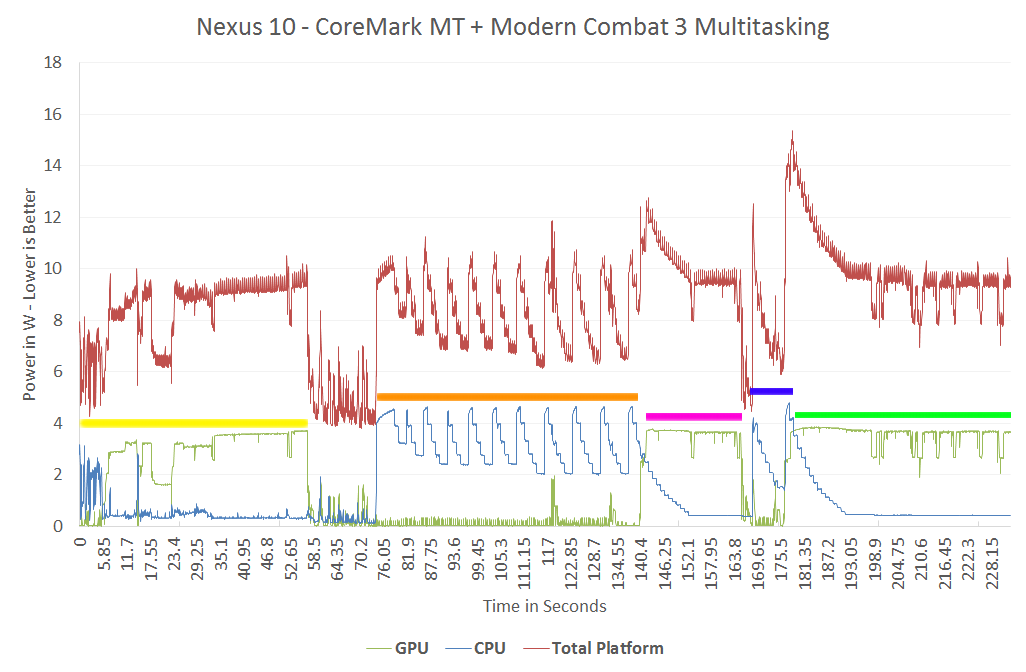
In the first section (yellow), we begin playing Modern Combat 3 - a GPU intensive first person shooter. GPU power consumption is just shy of 4W, while CPU power consumption remains below 1W. After about a minute of play we switch away from MC3 and you can see both CPU and GPU power consumption drop considerably. In the next section (orange), we fire up a multithreaded instance of CoreMark - a small CPU benchmark - and allow it to loop indefinitely. CPU power draw peaks at just over 4W, while GPU power consumption is understandably very low.
Next, while CoreMark is still running on both cores, we switch back to Modern Combat 3 (pink section of the graph). GPU voltage ramps way up, power consumption is around 4W, but note what happens to CPU power consumption. The CPU cores step down to a much lower voltage/frequency for the background task (~800MHz from 1.7GHz). Total SoC TDP jumps above 4W but the power controller quickly responds by reducing CPU voltage/frequency in order to keep things under control at ~4W. To confirm that CoreMark is still running, we then switch back to the benchmark (blue segment) and you see CPU performance ramps up as GPU performance winds down. Finally we switch back to MC3, combined CPU + GPU power is around 8W for a short period of time before the CPU is throttled.
Now this is a fairy contrived scenario, but it's necessary to understand the behavior of the Exynos 5250. The SoC is allowed to reach 8W, making that its max TDP by conventional definitions, but seems to strive for around 4W as its typical power under load. Why are these two numbers important? With Haswell, Intel has demonstrated interest (and ability) to deliver a part with an 8W TDP. In practice, Intel would need to deliver about half that to really fit into a device like the Nexus 10 but all of the sudden it seems a lot more feasible. Samsung hits 4W by throttling its CPU cores when both the CPU and GPU subsystems are being taxed, I wonder what an 8W Haswell would look like in a similar situation...


140 Comments
View All Comments
Kidster3001 - Friday, January 4, 2013 - link
Samsung uses everyone's chips in their phones. Samsung, Qualcomm, TI... everyone's. I would not be surprised to see a Samsung phone with Atom in it eventually.jeffkibuule - Friday, January 4, 2013 - link
They've never used other non-Samsung SoCs by choice, especially in their high end phones. They only used Qualcomm MSM8960 in the US GS III because Qualcomm's separate baseband MDM9615 wasn't ready. As soon as it was, we saw the Galaxy Note II use Exynos again. Nvidia and TI chips have been used in the low end from Samsung, but that's not profitable to anyone.Intel needs a major design win from a tier one OEM willing to put its chip inside their flagship phone, and with most phone OEMs actually choosing to start designing their own ARM SoCs (including even LG and Huawei), that task is getting a lot harder than you might think.
felixyang - Saturday, January 5, 2013 - link
some versions of Samsung's GS2 use TI's OMAP.iwod - Saturday, January 5, 2013 - link
Exactly like what is said above. If they have a choice they would rather use everything they produce themselves. Simply Because Wasted Fabs Space is expensive.Icehawk - Friday, January 4, 2013 - link
I find these articles very interesting - however I'd really like to see an aggregate score/total for power usage, IOW what is the area under the curve? As discussed being quicker to complete at higher power can be more efficient - however when looking at a graph it is very hard to see what the total area is. Giving a total wattage used during the test (ie, area under curve) would give a much easier metric to read and it is the important #, not what the voltage maxes or minimums at but the overall usage over time/process IMO.extide - Friday, January 4, 2013 - link
There are indeed several graphs that display total power used in joules, which is the area under the curve of the watts graphs. Maybe you missed them ?jwcalla - Friday, January 4, 2013 - link
That's what the bar charts are showing.GeorgeH - Friday, January 4, 2013 - link
It's already there. A Watt is a Joule/Second, so the area under the power/time graphs is measured in Watts * Seconds = Joules.Veteranv2 - Friday, January 4, 2013 - link
Another Intel PR Article, it is getting really sad on this website.Now since you are still using Win8 which is garbage for ARM. Please us the correct software platform for ARM chips. I'd love to see those power measurements then.
Anandtech did it again. Pick the most favorable software platform for Intel, give the least favorable to ARM.
Way to go! Again....
Intel PR at its best...
Veteranv2 - Friday, January 4, 2013 - link
Oh wait its even better!They used totally different screens with almost 4 times the pixels on the nexus 10 and then says it requires more power to do benchmarks. Hahaha, this review gave me a good laugh. Even worse then the previous ones.
This might explain the lack of product overviews at the start.