The ARM vs x86 Wars Have Begun: In-Depth Power Analysis of Atom, Krait & Cortex A15
by Anand Lal Shimpi on January 4, 2013 7:32 AM EST- Posted in
- Tablets
- Intel
- Samsung
- Arm
- Cortex A15
- Smartphones
- Mobile
- SoCs
Determining the TDP of Exynos 5 Dual
Throughout all of our Cortex A15 testing we kept bumping into that 4W ceiling with both the CPU and GPU - but we rarely saw both blocks use that much power at the same time. Intel actually tipped me off to this test to find out what happens if we try and force both the CPU and GPU to run at max performance at the same time. The graph below is divided into five distinct sections, denoted by colored bars above the sections. On this chart I have individual lines for GPU power consumption (green), CPU power consumption (blue) and total platform power consumption, including display, measured at the battery (red).
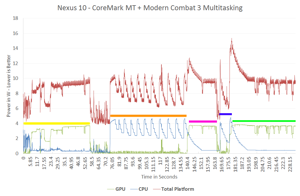
In the first section (yellow), we begin playing Modern Combat 3 - a GPU intensive first person shooter. GPU power consumption is just shy of 4W, while CPU power consumption remains below 1W. After about a minute of play we switch away from MC3 and you can see both CPU and GPU power consumption drop considerably. In the next section (orange), we fire up a multithreaded instance of CoreMark - a small CPU benchmark - and allow it to loop indefinitely. CPU power draw peaks at just over 4W, while GPU power consumption is understandably very low.
Next, while CoreMark is still running on both cores, we switch back to Modern Combat 3 (pink section of the graph). GPU voltage ramps way up, power consumption is around 4W, but note what happens to CPU power consumption. The CPU cores step down to a much lower voltage/frequency for the background task (~800MHz from 1.7GHz). Total SoC TDP jumps above 4W but the power controller quickly responds by reducing CPU voltage/frequency in order to keep things under control at ~4W. To confirm that CoreMark is still running, we then switch back to the benchmark (blue segment) and you see CPU performance ramps up as GPU performance winds down. Finally we switch back to MC3, combined CPU + GPU power is around 8W for a short period of time before the CPU is throttled.
Now this is a fairy contrived scenario, but it's necessary to understand the behavior of the Exynos 5250. The SoC is allowed to reach 8W, making that its max TDP by conventional definitions, but seems to strive for around 4W as its typical power under load. Why are these two numbers important? With Haswell, Intel has demonstrated interest (and ability) to deliver a part with an 8W TDP. In practice, Intel would need to deliver about half that to really fit into a device like the Nexus 10 but all of the sudden it seems a lot more feasible. Samsung hits 4W by throttling its CPU cores when both the CPU and GPU subsystems are being taxed, I wonder what an 8W Haswell would look like in a similar situation...


140 Comments
View All Comments
StrangerGuy - Sunday, March 24, 2013 - link
You really think having a slightly better chip would make Samsung risk everything to get locked into a chip with an ISA owned, designed and manufactured by one single sole supplier? And when that supplier in question historically has shown all sorts of monopolistic abuses?And when a quad A7 could already scroll desktop sites in Android capped at 60 fps additional performance provides very little real world advantage for most users. I'll even say most users would be annoyed by I/O bottlenecks like LTE speeds long before saying 2012+ class ARM CPUs are too slow.
duploxxx - Monday, January 7, 2013 - link
Now it is clear that when Intel provides that much material and resources that they know they are at least ok in the comapere against ARM on cpu and power... else they wouldn't make such a fuss...,but what about GPU? any decent benchmark or testing available on GPU performance.
I played in december with HP envy2 and after some questioning they installed a few light games which were "ok" but i wonder how well the gpu in the atom really is, power consumption looks ok, but i preffer a performing gpu @ a bit higher power then a none performing one.
memosk - Tuesday, January 8, 2013 - link
It looks like old problem with PowerPc v.s. PC .PowerPC have had a faster Risc procesor and PC have had slower x86 like procesor .
The end result was that clasical PC has won this Battle . Because of tradition and what is more important , you need knowledge about platform over users, producers, programers ...
And you should think about economical thinks like mortage and whole enviroment named as Logistik.
The same problem was Tesla vs. Edison. Tesla have had better ideas and Edison was Bussines-man. Who has won ? :)
memosk - Tuesday, January 8, 2013 - link
Nokia tryed seriosly sell windows 8 phones without SD cards And they said because of microsoft .How can you then compete again android with SD cards. But if you copy an Apple you think it has logic.
You need generaly: complete and logic and OWN and CONSISTENT and ORIGINAL strategy.
If you copy something it is dangerous that you strategy will be incostintent , leaky , "two way" , vague also with tragical errors like incompatibility or like legendary siemens phones: 1 crash per day . :D
apozean - Friday, January 11, 2013 - link
I studied the setup and it appears and Intel just wants to take on Nvidia's Tegra 3. Here are a couple of differences that I think are not highlighted appropriately:1. They used an Android tablet for Atom, Android tablet for Krait, but a Win RT (Surface) for Tegra 3. It must have been very difficult to fund a Google Nexus 7. Keeping the same OS across the devices would have controlled for a lot of other variables. Wouldn't it?
2. Tegra 3 is the only quad core chip among chips being compared. Atom and Krait are dual-core. If all four cores are running, wouldn't it make a different to the idle power?
3. Tegra 3 is built on 40nm and is one of the first A9 SoCs. In contrast, Atom is 32nm and Krait is 28nm.
How does Tegra 3 fits in this setup?
apozean - Friday, January 11, 2013 - link
Fixing typos..I studied the setup and it appears that Intel just wants to take on Nvidia's Tegra 3. Here are a couple of differences that I think are not highlighted appropriately:
1. They used an Android tablet for Atom, Android tablet for Krait, but a Win RT (Surface) for Tegra 3. It must have been very difficult to fund a Google Nexus 7. Keeping the same OS across the devices would have controlled for a lot of other system variables. Wouldn't it?
2. Tegra 3 is the only quad core chip among chips being compared. Atom and Krait are dual-core. If all four cores are running, wouldn't it make a difference to the idle power?
3. Tegra 3 is built on 40nm and is one of the first A9 SoCs. In contrast, Atom is 32nm and Krait is 28nm.
How does Tegra 3 fit in this setup?
some_guy - Wednesday, January 16, 2013 - link
I thinking this may be the beginning of Intel being commoditied and the end of the juicy margins for most of their sales.I was just reading an article about how hedge funds love Intel. I don't see it, but that doesn't mean that the hedge funds would make money. Perhaps they know the earning report that is coming out soon, maybe tomorrow, will be good. http://www.insidermonkey.com/blog/top-semiconducto...
some_guy - Wednesday, January 16, 2013 - link
I meant to say "but that doesn't mean that the hedge funds won't make money."raptorious - Wednesday, February 20, 2013 - link
but Anand has no clue what the rails might actually be powering. How do we know that the "GPU Rail" is in fact just powering the GPU and not the entire uncore of the SOC? This article is completely biased towards Intel and lacks true engineering rigor.EtTch - Tuesday, April 2, 2013 - link
My take in all of this is that ARM and x86 is in comparable at this point when it comes to comparing the different instruction set architectures due to different the lithography size and the new 3d transistors. When ARM based SOC has finally all the physical features of the x86 then it's only truly comparable. Right now x86 is most likely to have a lower power consumption than ARM based processors that has a higher lithographic size than itself. (I really don't know what it's called but I'll go out on a limb and call it lithography size even though I know that I am most likely wrong)