AMD Announces Their First 8000M GPUs
by Jarred Walton on December 17, 2012 4:21 PM ESTAMD held a press briefing today on their upcoming 8000M graphics chips, which they are calling the "second generation GCN architecture" parts. We’ll have more on that in a moment, but while we were expecting (dreading) a rebranding prior to the call, it appears we are at least partially mistaken; there will be at least one completely new GPU with 8000M. (If you want additional background material, you can see the previous generation high-end 7000M announcement from April 2012 for reference.)
I’m not going to get too far into the marketing aspects, as we’ve heard all of this information before: AMD has improved Enduro Technology, they’re continuing to improve their drivers, and APP Acceleration has a few more applications. There have been a few major titles released in the past couple of months with AMD Gaming Evolved branding (Far Cry 3 is arguably the most notable of the offerings, with Hitman: Absolution and Sleeping Dogs also scoring well amongst critics and users), and Bioshock Infinite is at least one future release that I'm looking forward to playing.
Cutting straight to the chase, at this point AMD has released limited information on the core specifications for some of their 8000M GPUs, but they coyly note that at least one more GPU announcement will be forthcoming in Q2 2013 (8900M by all appearances). Today is a soft launch of high level details, with more architectural information and product details scheduled for January 7, 2013 at CES. AMD did not share any codenames for the newly announced mobile GPUs, if you’re wondering, other than the overall family name of “Solar” for the mobile chips (replacing the outgoing “London” series), but we do know from other sources that the 384 core part is codenamed "Mars" while the larger 640 core part is codenamed "Neptune". Here are the details we have right now:
| AMD Radeon HD 8500M, 8600M, 8700M, and 8800M | ||||
|
Radeon HD 8500M |
Radeon HD 8600M |
Radeon HD 8700M |
Radeon HD 8800M |
|
| Stream Processors | 384 | 384 | 384 | 640 |
| Engine Clock | 650MHz | 775MHz | 650-850MHz | 650-700MHz |
| Memory Clock | 2.0GHz/4.5GHz | 2.0GHz/4.5GHz | 2.0GHz/4.5GHz | 4.5GHz |
| Memory Type | DDR3/GDDR5 | DDR3/GDDR5 | DDR3/GDDR5 | GDDR5 |
| FP32 GFLOPS | 537 | 633 | 537-691 | 992 |
| FP64 GFLOPS | 33 | 39 | 33-42 | 62 |
Obviously there are a lot of missing pieces right now, but what we immediately notice is that the core count on the 8500M/8600M/8700M means that we’re definitely looking at a new GPU. The only other time we’ve seen AMD do 384 cores is with Trinity, but that’s a VLIW4 architecture so we’re not seeing that again. Given the currently shipping Southern Islands chips (“London” on the mobile side) have 640 cores max for Cape Verde, 1280 max for Pitcairn, and up to 2048 for Tahiti, AMD has likely created a fourth SI derivative that drops down to two CU arrays, each with three CUs. (You can read more about the GCN/SI architecture in our earlier GPU coverage.) Performance is something of a wildcard with the new 384 core parts, and the choice of DDR3/GDDR5 memory will also influence the final result. We'll find out in the coming months how the 8500/8600/8700M stack up to NVIDIA's midrange "GT" offerings, which interestingly are also using 384 cores.
Also worth a quick note is that AMD is not discussing TDPs at this point in time—which is common practice for both AMD and NVIDIA. We expect the new "Mars" parts to be more power efficient than the outgoing Thames/Turks cores, thanks to the shrink to a 28nm process. However, AMD and NVIDIA typically stick to common power targets for laptops that are dictated by their OEM partners, which often means they'll play with clock speeds in order to hit a specific TDP. That's why all of the clock speeds listed in the above table have a qualifying "up to" prefix (which I omitted).
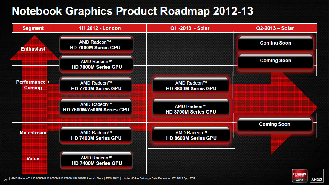
The final announced card is the one where we appear to have more of a rebrand/optimization of a previous generation chip. 8800M has the same 640 core count as Cape Verde/7800M, only with modified clocks this time. The earlier 7800M chips could clock up as high as 800MHz, so maximum core clock is actually down a bit, but they only ran the memory at up to 1GHz (4GHz effective) GDDR5. If AMD determined memory bandwidth was more important for that particular GPU than shader performance, the new 8800M would make sense. Also note that AMD isn’t including the boost clock speeds into the above chart; under the right circumstances, all of the new chips can run at higher clocks than the reference clock.
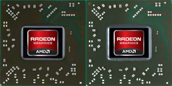
Radeon 7800M Left, Radeon 8800M Right
AMD isn’t calling the 8800M a rebrand, but we’re looking at the same core counts as Cape Verde and the same 28nm process technology, so we wouldn’t expect a substantial change in performance. There’s also the above chip shot as a point of reference. If the 8800M is substantially different from Cape Verde then the above images provided in AMD’s slides must be incorrect, as the new and old chips look the same. Minor tweaks to power use, caching, or other elements notwithstanding, we’re probably dealing with a die respin at most. But, there’s nothing inherently wrong with rebranding—AMD and NVIDIA have both been doing it for some time now. Don’t expect every “upgraded” GPU to be better; a 7400M isn’t faster than a 6700M, and likewise we expect 7700M and 7800M to be faster options than the 384 core 8500M/8600M/8700M and competitive with 8800M. Here’s a quick recap of the same core specs as above for the current 7700M/7800M parts:
| AMD Radeon HD 7700M/7800M Specifications | |||||
|
Radeon HD 7730M |
Radeon HD 7750M |
Radeon HD 7770M |
Radeon HD 7850M |
Radeon HD 7870M |
|
| Stream Processors | 512 | 512 | 512 | 640 | 640 |
| Engine Clock | 575-675MHz | 575MHz | 675MHz | 675MHz | 800MHz |
| Memory Clock | 1.8GHz | 4.0GHz | 4.0GHz | 4.0GHz | 4.0GHz |
| Memory Type | DDR3 | GDDR5 | GDDR5 | GDDR5 | GDDR5 |
| FP32 GFLOPS | 589-691 | 589 | 691 | 864 | 1024 |
| FP64 GFLOPS | 36.8-43.2 | 36.8 | 43.2 | 54 | 64 |
I’ll refrain from commenting too much more about performance of an unreleased part, but AMD indicated their 8870M should be substantially faster than NVIDIA’s current GT 650M GDDR5 (which isn’t too surprising considering clocks and core counts), and the 8770M should likewise be a healthy 20%+ bump in performance relative to the 7670M. I’d rather see comparisons with GTX 670MX and HD 7770M, respectively, but I suspect those wouldn’t be quite as impressive. Anyway, you can see AMD’s comparison charts in the complete slide deck gallery below. Availability of the new GPUs is slated for Q1 2013.


88 Comments
View All Comments
Zodiark1593 - Saturday, December 22, 2012 - link
You do realize that Nvidia is equally guilty for botched naming schemes and rebranding as well?Anyway, the arguing should stop. I thank Jarrod for sharing his opinions, and letting us know about the soft launch.
On both fronts, I find the naming scheme from both AMD and Nvidia equally convoluted for mobile GPUs. In my opinion, I think it's partially the names that help turn people off from PC gaming. Unless one is well versed beforehand, how is one supposed to know a Radeon 7800 chip curb stomps the 8500M. Certainly a salesman won't tell you which is what, and Joe Average would probably buy his aspiring gamer kid the laptop with an 8500M as it's a higher number.
Retailers should step up to the plate here and help the customer differentiate the numbers, but they seem more content on keeping things pretty cryptic as well. How I wish I owned my own retailer...
CeriseCogburn - Tuesday, December 25, 2012 - link
Do you realize i was refuting mrdude's bs post ?Do you realize this is an amd article ?
Frankly all the whining about rebranding makes me LOL.
We have all these pinheads who pretend they are techs or intelligent, but a few card numbers throw them into a hellspin they cannot handle
They aren't bright at all, so of course they always claim they are complaining to protect the "general consumer" they never met and never will meet. LOL
I've never seen such pathetic liars in my entire life.
Hows that for some reality ? You like that ?
Here's some more, the idiots always complaining no doubt go out half cocked or doped up and buy the wrong thing, near constantly.
LOL
There's reality. It's not the ephemeral consumer, it's their own stupid butt that's in a sling - they won't be able to remember much of anything once it's time to buy.
That's the real problem.
CaptainDoug - Monday, December 17, 2012 - link
So I assume we don't know anything about about the power consumption yet right?iwod - Tuesday, December 18, 2012 - link
I dont remember the code names anymore, Everyone makes them so hard to remember especially AMD. ( And i think that is part of the reason why they dont generate Hype well at all )So the 7xxx Series on Desktop was based on GCN, which is AMD's first serious attempt to focus more on compute rather then graphics, and reason why Kelper were faster graphics wise.
The 7xxx on Mobile were basically a rebrand from 6xxx series. The new 8xxx Mobile is actually just GCN from Desktop. Which was actually released a year ago.
Please correct me if I am wrong because i am lost and that is what comprehend.
But then the confusion part is "second generation GCN architecture" . Wasn't the 7xxx series on Desktop a First Gen GCN?
Ryan Smith - Tuesday, December 18, 2012 - link
It's a bit more complex than that.The first, low-end 7000M parts were rebadges of last-generation 40nm VLIW5 GPUs (specifically Turks and Caicos). These were introduced right at the start of 2012 so that AMD would have a fresh product line for OEMs (who hate selling the same thing 2 years in a row). So the 7400M, 7500M, and 7600M were all rebadges.
http://www.anandtech.com/show/5200/introducing-amd...
A few months later AMD introduced mobile parts based on their new 28nm Southern Islands GPUs; the 7700M, 7800M, and 7900M. These existed alongside the earlier VLIW5 GPUs. So it is wrong to say that the 7000M was composed of just rebadges, as it contained some GCN parts.
http://www.anandtech.com/show/5778/amd-launches-ra...
The 8000M series will shape up similarly to the 7000M series. It will be a mix of 2012 GPUs (today's announcement) and 2013 GPUs that will be launched a couple of quarters from now.
As for the second generation comment, that appears to be AMD being generous to itself. We don't have the full details on the new GPU being used to make these low-end parts, but so far it appears to functionally be a very late member of Southern Islands rather than a SI-successor.
iwod - Tuesday, December 18, 2012 - link
Thx, that makes much more sense and i record now there were indeed 28nm 7xxx mobile GPU... yes i forgot, and mixed up.But unlike the previous announcement where 7400 and 7600 are using lower numbers for previous generation , and reserving the 7700 - 7900 for newer parts, this time around AMD actually uses it all the way up to 8800.
May be i have to wait for more details to come. But that makes today's announcement TOTALLY pointless, and far too early. They will disappoint ( again ) if they dont really a SI-successor, and i seriously doubt they do.
Death666Angel - Tuesday, December 18, 2012 - link
"But, there’s nothing inherently wrong with rebranding—AMD and NVIDIA have both been doing it for some time now."Yes it is inherently wrong, because it is misleading the customer. Just because they have been doing it for a while does not make it better or acceptable.
Mr Perfect - Tuesday, December 18, 2012 - link
Agreed, rebadging is sleazy. They'll both keep doing it though.CeriseCogburn - Wednesday, December 19, 2012 - link
NO, AMD did it here.It's amd whom has done it.
AMD is guilty.
AMD
That's
Who
Just
Did
It
Nice you fanboys cannot help blaming the competition when amd craps all over you.
silverblue - Thursday, December 20, 2012 - link
Oh, I cannot WAIT for the 7xx series, mobile or otherwise.From Wikipedia:
2 The GeForce 605 (OEM) card is a rebranded GeForce 510.
3 The GeForce GT 610 card is a rebranded GeForce GT 520.
4 The GeForce GT 620 (OEM) card is a rebranded GeForce GT 520.
5 The GeForce GT 620 card is a rebranded GeForce GT 530.
6 The GeForce GT 630 (DDR3) card is a rebranded GeForce GT 440 (DDR3).
7 The GeForce GT 630 (GDDR5) card is a rebranded GeForce GT 540 (GDDR5).
8 The GeForce GT 640 (OEM) card is a rebranded GeForce GT 545 (DDR3).
9 The GeForce GT 645 (OEM) card is a rebranded GeForce GTX 560 SE.
Additionally, let's look at the 600M series.
610M - Fermi
620M - Fermi
625M - Fermi
630M - Fermi
635M - Fermi
640M LE - BOTH
640M - Kepler
645M - Kepler
650M - Kepler
660M - Kepler
670M - Fermi
670MX - Kepler
675M - Fermi
675MX - Kepler
680M - Kepler
680MX - Kepler
There's a subtle difference between AMD and NVIDIA here - AMD's higher end parts are all GCN whereas their lower parts are the previous mainstream generation. This has advantages (simplified product stack - you know what series you're getting above or below a certain point) and disadvantages (older tech at lower price points - less current tech or higher power usage). At no point are there two AMD products with the same number and different architectures, where there are two instances of this with NVIDIA - the 640M LE and the 640. Also of note is the 630 which is a rebranded 440 - TWO product lines back.
Let's face facts here - both companies bring their previous generation over to fill their current product lines. If you're IT literate enough, you won't get too confused. I just happen to think that it's a little clearer which series you're getting with AMD, but it's debatable whether you're getting better performance with comparable model numbers from one series to the next in some cases. NVIDIA does seem more consistent with offering better performance between, say, x60 products, though far more so on the desktop.
Buy what you want. Right now, comparing GCN to Kepler, NVIDIA has the more efficient gaming architecture, however they started a revolution in compute that they look to have backed away from.