NVIDIA Launches Tesla K20 & K20X: GK110 Arrives At Last
by Ryan Smith on November 12, 2012 9:00 AM ESTGK110: The GPU Behind Tesla K20
Now that we’ve discussed the Telsa K20 series from the big-picture perspective of performance, configurations, pricing, and the marketplace, we can finally dive into the technical underpinnings of the K20.
Announced alongside the Tesla K20 back at NVIDIA’s GTC 2012 was the GPU that would be powering it: GK110. In a reversal of their usual pattern, GK110 was to be NVIDIA’s first compute-oriented Kepler GPU (GK10X having been significantly stripped for gaming efficiency purposes), but it would be the last Kepler GPU to launch. Whereas in the Fermi generation we saw GF100 first and could draw some conclusions about the eventual Tesla cards from that, GK110 has been a true blank slate. On the other hand because it builds upon NVIDIA’s earlier Kepler GPUs, we can draw a clear progression from GK104 to GK110.
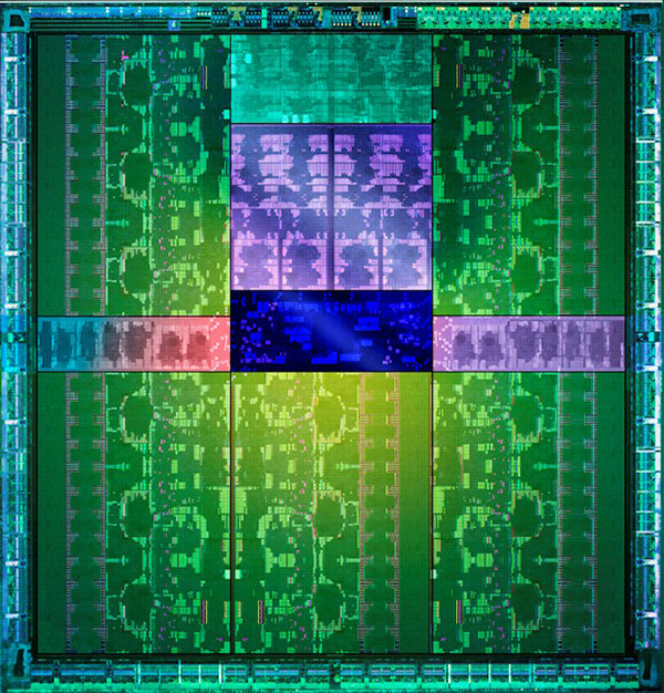
GK110 is NVIDIA’s obligatory big-die GPU. We don’t have a specific die size, but at 7.1 billion transistors it is now the biggest GPU ever built in terms of transistors, dwarfing the 3.5B transistor GK104 and the 4.3B transistor Tahiti GPU from AMD. These big-die GPUs are unwieldy from a fabrication and power consumption perspective, but the end result is that the performance per GPU is unrivaled due to the fact that so many tasks (both graphical and compute) are embarrassingly parallel and map well to the large arrays of streaming processors found in a GPU.
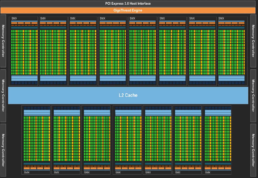
Like GF100 before it, GK110 has been built to fill multiple roles. For today’s launch we’re mostly talking about it from a compute perspective – and indeed most of the die is tied up compute hardware – but it also has all of the graphics hardware we would expect in an NVIDIA GPU. Altogether it packs 15 SMXes and 6 ROP/L2/memory controller blocks, versus 8 SMXes and 4 ROP/L2/memory blocks on GK104. Not accounting for clockspeeds this gives GK110 87% more compute performance and 50% more memory bandwidth than GK104. But there’s a great deal more to GK110 than just a much larger collection of functional units.
| NVIDIA GPU Comparison | ||||||
| Fermi GF100 | Fermi GF104 | Kepler GK104 | Kepler GK110 | |||
| Compute Capability | 2.0 | 2.1 | 3.0 | 3.5 | ||
| Threads/Warp | 32 | 32 | 32 | 32 | ||
| Max Warps/SM(X) | 48 | 48 | 64 | 64 | ||
| Max Threads/SM(X) | 1536 | 1536 | 2048 | 2048 | ||
| Register File | 32,768 | 32,768 | 65,536 | 65,536 | ||
| Max Registers/Thread | 63 | 63 | 63 | 255 | ||
| Shared Mem Config |
16K 48K |
16K 48K |
16K 32K 48K |
16K 32K 48K |
||
| Hyper-Q | No | No | No | Yes | ||
| Dynamic Parallelism | No | No | No | Yes | ||
Fundamentally GK110 is a highly enhanced if not equally specialized version of the Kepler architecture. The SMX, first introduced with GK104, is the basis of GK110. Each GK104 SMX contained 192 FP32 CUDA cores, 8 FP64 CUDA cores, 256KB of register file space, 64KB of L1 cache, 48KB of uniform cache. In turn it was fed by 4 warp schedulers, each with two dispatch units, allowing GK104 to issue instructions from warps in a superscalar manner.
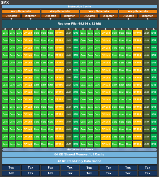
GK110 SMX
GK110 builds on that by keeping the same general design, but tweaking it for GK110’s compute-focused needs. The single biggest change here is that rather than 8 FP64 CUDA cores GK110 has 64 FP64 CUDA cores, giving it 8 times the FP64 performance of a GK104 SMX. The SMXes are otherwise very similar at a high level, featuring the same 256KB of register file space, 64KB of L1 cache, 48KB of uniform cache, and the same warp scheduler structure. This of course does not include a number of low level changes that further set apart GK104 and GK110.
Meanwhile this comparison gets much more jarring if we take a look at GK110 versus GF100 and by extension Tesla K20 versus its direct predecessors, the Fermi based Tesla family. The GK110 SMX compared to the GF100 SM is nothing short of a massive change. Superficially NVIDIA has packed many more CUDA cores into an SMX than they have an SM due to the change from a shader design that ran fewer CUDA cores at a very high (double pumped) clockspeed to a design that runs many more CUDA cores at a lower (single pumped) clockspeed, but they also have changed their warp execution model on its head in the process.

GF100/GF110 SM
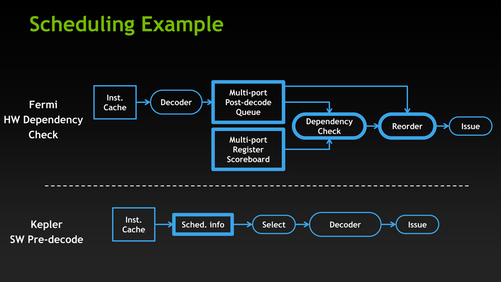
GF100 was essentially a thread level parallelism design, with each SM executing a single instruction from up to two warps. At the same time certain math instructions had variable latencies, so GF100 utilized a complex hardware scoreboard to do the necessary scheduling. Compared to that, GK110 introduces instruction level parallelism to the mix, making the GPU reliant on a mix of high TLP and high ILP to achieve maximum performance. The GPU now executes from 4 warps, ultimately executing up to 8 instructions at once if all of the warps have ILP-suitable instructions waiting. At the same time scheduling has been moved from hardware to software, with NVIDIA’s compiler now statically scheduling warps thanks to the fact that every math instruction now has a fixed latency. Finally, to further improve SMX utilization FP64 instructions can now be paired with other instructions, whereas on GF100 they had to be done on their own.
The end result is that at an execution level NVIDIA has sacrificed some of GF100’s performance consistency by introducing superscalar execution – and ultimately becoming reliant on it for maximum performance. At the same time they have introduced a new type of consistency (and removed a level of complexity) by moving to fixed latency instructions and a static scheduled compiler. Thankfully a ton of these details are abstracted from programmers and handled by NVIDIA’s compiler, but for HPC users who are used to getting their hands dirty with low level code they are going to find that GK110 is more different than it would seem at first glance.
With that said, even with the significant changes to their warp execution model, GK110 brings more changes yet. We can’t hope to replicate the sheer amount of depth NVIDIA’s own GK110 whitepaper covers, but there are several other low-level changes that further separate GK110 from GF100.
Space and bandwidth for both the register file and the L2 cache have been greatly increased for GK110. At the SMX level GK110 has 256KB of register file space, composed of 65K 32bit registers, as compared to 128KB of such space (32K registers) on GF100. Bandwidth to those register files has in turn been doubled, allowing GK110 to read from those register files faster than ever before. As for the L2 cache, it has received a very similar treatment. GK110 uses an L2 cache up to 1.5MB, twice as big as GF110; and that L2 cache bandwidth has also been doubled.
What makes this all the more interesting is that while NVIDIA significantly increased the number of CUDA cores in an SM(X), in fact by far more than the increase in cache and register file sizes, they only marginally increased the number of threads that are actually active on an SMX. Each GK110 SMX can only have up to 2K threads at any time, 1.33x that of GF100 and its 1.5K threads. So as a result GK110 is working from a thread pool only slightly larger than what GF100 worked with, which means that despite the increase in CUDA cores they actually improve their performance in register-starved scenarios as there are more registers available to each thread. This goes hand in hand with an increase in the total number of registers each thread can address, moving from 63 registers per thread on GF100 to 255 registers per thread with GK110.
While we’re on the subject of caches, it’s also worth noting that NVIDIA has reworked their texture cache to be more useful for compute. On GF100 the 12KB texture cache was just that, a texture cache, only available to the texture units. As it turns out, clever programmers were using the texture cache as another data cache by mapping normal data at texture data, so NVIDIA has promoted the texture cache to a larger, more capable cache on GK110. Now measuring 48KB in size, in compute mode the texture cache becomes a read-only cache, specializing in unaligned memory access patterns. Furthermore error detection capabilities have been added to it to make it safer for use with workloads that rely on ECC.
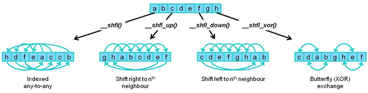
Last, but certainly not least in our low level look, NVIDIA has added a number of new instructions and operations to GK110 to further improve performance. New shuffle instructions allow for threads within a warp to share (i.e. shuffle) data without going to shared memory, making the process much faster than the old load/share/store method. Meanwhile atomic operations have also been overhauled, with NVIDIA both speeding up the execution speed of atomic operations and adding some FP64 operations that were previously only available for FP32 data.


73 Comments
View All Comments
dcollins - Monday, November 12, 2012 - link
It should be noted that recursive algorithms are not always more difficult to understand than their iterative counterparts. For example, the quicksort algorithm used in nvidia's demos is extremely simple to implement recursively but somewhat tricky to get right with loops.The ability to directly spawn sub-kernels has applications beyond supporting recursive GPU programming. I could see the ability to create your own workers would simplify some problems and leave the CPU free to do other work. Imagine an image processing problem where a GPU kernel could do the work of sharding an image and distributing it to local workers instead of relying on a (comparatively) distant CPU to perform that task.
In the end, this gives more flexibility to GPU compute programs which will eventually allow them to solve more problems, more efficiently.
mayankleoboy1 - Monday, November 12, 2012 - link
We need compilers that can work on GPGPU to massively speed up compilation times.Loki726 - Tuesday, November 13, 2012 - link
I'm working on this. It actually isn't as hard as it might seem at first glance.The amount of parallelism in many compiler optimizations scale with program size, and the simplest algorithms basically boil down to for(all instructions/functions/etc) { do something; }. Everything isn't so simple though, and it still isn't clear if there are parallel versions of some algorithms that are as efficient as their sequential implementations (value-numbering is a good example).
So far the following work very well on a massively parallel processor:
- instruction selection
- dataflow analysis (live sets, reaching defs)
- control flow analysis
- dominance analysis
- static single assignment conversion
- linear scan register allocation
- strength reduction, instruction simplification
- constant propagation (local)
- control flow simplification
These are a bit harder and need more work:
- register allocation (general)
- instruction scheduling
- instruction subgraph isomorphism (more general instruction selection)
- subexpression elimination/value numbering
- loop analysis
- alias analysis
- constant propagation (global)
- others
Some of these might end up being easy, but I just haven't gotten to them yet.
The language frontend would also require a lot of work. It has been shown
that it is possible to parallelize parsing, but writing a parallel parser for a language
like C++ would be a very challenging software design project. It would probably make more sense to build a parallel parser generator for framework like Bison or ANTLR than to do it by hand.
eachus - Wednesday, November 14, 2012 - link
I've always assumed that the way to do compiles on a GPU or other heavily parallel CPU is to do the parsing in a single sequential process, then spread the semantic analysis and code generation over as many threads as you can.I may be biased in this since I've done a lot of work with Ada, where adding (or changing) a 10 line file can cause hundreds of re-analysis/code-generation tasks. The same thing can happen in any object-oriented language. A change to a class library, even just adding another entry point, can cause all units that depend on the class to be recompiled to some extent. In Ada you can often bypass the parser, but there are gotchas when the new function has the same (simple) name as an existing function, but a different profile.
Anyway, most Ada compilers, including the GNAT front-end for GCC will use as many CPU cores as are available. However, I don't know of any compiler yet that uses GPUs.
Loki726 - Thursday, November 15, 2012 - link
The language frontend (semantic analysis and IR generation, not just parsing) for C++ is generally harder than languages that have concepts of import/modules or interfaces because you typically need to parse all included files for every object file. This is especially true for big code bases (with template libraries).GPUs need thousands of way parallelism rather than just one dimension for each file/object, so it is necessary to extract parallelism on a much finer granularity (e.g. for each instruction/value).
A major part of the reason why GPU compilers don't exist is because they are typically large/complex codebases that don't map well onto parallel models like OpenMP/OpenACC etc. The compilers for many languages like OpenCL are also immature enough that writing a debugging a large codebase like this would be intractable.
CUDA is about the only language right now that is stable enough and has enough language features (dynamic memory allocation, object oriented programming, template) to try. I'm writing all of the code in C++ right now and hoping that CUDA will eventually cease to be a restricted subset of C++ and just become C++ (all it is missing is exceptions, the standard library, and some minor features that other compilers are also lax about supporting).
CeriseCogburn - Thursday, November 29, 2012 - link
Don't let the AMD fans see that about OpenCL sucking so badly and being immature.It's their holy grail of hatred against nVidia/Cuda.
You might want to hire some protection.
I can only say it's no surprise to me, as the amd fanboys are idiots 100% of the time.
Now as amd crashes completely, gets stuffed in a bankruptcy, gets dismantled and bought up as it's engineers are even now being pillaged and fired, the sorry amd fanboy has "no drivers" to look forward to.
I sure hope their 3G ram 79xx "futureproof investment" they wailed and moaned about being the way to go for months on end will work with the new games...no new drivers... 3rd tier loser engineers , sparse crew, no donuts and coffee...
*snickering madly*
The last laugh is coming, justice will be served !
I'd just like to thank all the radeon amd ragers here for all the years of lies and spinning and amd tokus kissing, the giant suction cup that is your pieholes writ large will soon be able to draw a fresh breath of air, you'll need it to feed all those delicious tears.
ROFL
I think I'll write the second edition of "The Joys of Living".
inaphasia - Tuesday, November 13, 2012 - link
Everybody seems to be fixated on the fact that the K20 doesn't have ALL it's SMXes enabled and assuming this is the result of binning/poor yields, whatever...AFAICT the question everybody should be asking and the one I'd love to know the answer to is:
Why does the TFLOP/W ratio actually IMPROVE when nVidia does that?
Watt for Watt the 660Ti is slightly better at compute than the 680 and far better than the 670, and we all know they are based on the "same" GK104 chip. Why? How?
My theory is that even if TSCM's output of the GK110 was golden, we'd still be looking at disabled SMXes. Of course since it's just a theory, it could very well be wrong.
frenchy_2001 - Tuesday, November 13, 2012 - link
No, you are probably right.Products are more than their raw capabilities. When GF100 came out, Nvidia placed a 480 core version (out of 512) in the consumer market (at 700MHz+) and a 448 at 575MHz in the Quadro 6000. Power consumption, reliability and longevity were all parts of that decision.
This is part of what was highlighted in the article as a difference between K20X and K20, the 235W vs 225W makes a big difference if your chassis is designed for the latter.
Harry Lloyd - Tuesday, November 13, 2012 - link
Can you actually play games with these cards (drivers)?I reckon some enthusiasts would pick this up.
Ryan Smith - Wednesday, November 14, 2012 - link
Unfortunately not. If nothing else, because there aren't any display outputs.