NVIDIA Launches Tesla K20 & K20X: GK110 Arrives At Last
by Ryan Smith on November 12, 2012 9:00 AM ESTGK110: The GPU Behind Tesla K20
Now that we’ve discussed the Telsa K20 series from the big-picture perspective of performance, configurations, pricing, and the marketplace, we can finally dive into the technical underpinnings of the K20.
Announced alongside the Tesla K20 back at NVIDIA’s GTC 2012 was the GPU that would be powering it: GK110. In a reversal of their usual pattern, GK110 was to be NVIDIA’s first compute-oriented Kepler GPU (GK10X having been significantly stripped for gaming efficiency purposes), but it would be the last Kepler GPU to launch. Whereas in the Fermi generation we saw GF100 first and could draw some conclusions about the eventual Tesla cards from that, GK110 has been a true blank slate. On the other hand because it builds upon NVIDIA’s earlier Kepler GPUs, we can draw a clear progression from GK104 to GK110.
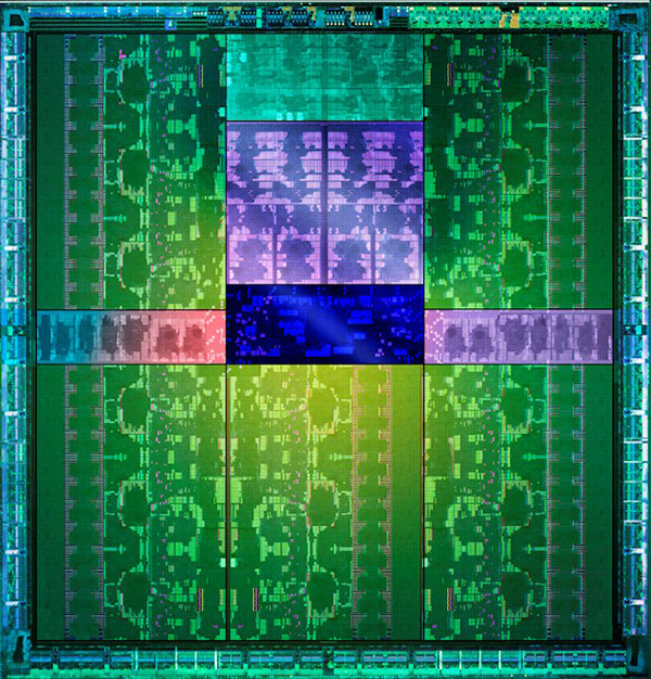
GK110 is NVIDIA’s obligatory big-die GPU. We don’t have a specific die size, but at 7.1 billion transistors it is now the biggest GPU ever built in terms of transistors, dwarfing the 3.5B transistor GK104 and the 4.3B transistor Tahiti GPU from AMD. These big-die GPUs are unwieldy from a fabrication and power consumption perspective, but the end result is that the performance per GPU is unrivaled due to the fact that so many tasks (both graphical and compute) are embarrassingly parallel and map well to the large arrays of streaming processors found in a GPU.
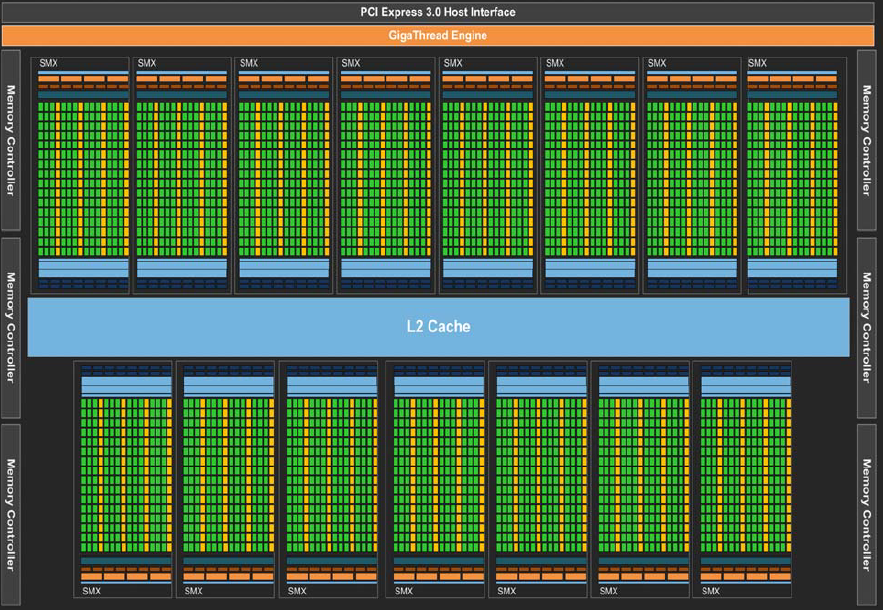
Like GF100 before it, GK110 has been built to fill multiple roles. For today’s launch we’re mostly talking about it from a compute perspective – and indeed most of the die is tied up compute hardware – but it also has all of the graphics hardware we would expect in an NVIDIA GPU. Altogether it packs 15 SMXes and 6 ROP/L2/memory controller blocks, versus 8 SMXes and 4 ROP/L2/memory blocks on GK104. Not accounting for clockspeeds this gives GK110 87% more compute performance and 50% more memory bandwidth than GK104. But there’s a great deal more to GK110 than just a much larger collection of functional units.
| NVIDIA GPU Comparison | ||||||
| Fermi GF100 | Fermi GF104 | Kepler GK104 | Kepler GK110 | |||
| Compute Capability | 2.0 | 2.1 | 3.0 | 3.5 | ||
| Threads/Warp | 32 | 32 | 32 | 32 | ||
| Max Warps/SM(X) | 48 | 48 | 64 | 64 | ||
| Max Threads/SM(X) | 1536 | 1536 | 2048 | 2048 | ||
| Register File | 32,768 | 32,768 | 65,536 | 65,536 | ||
| Max Registers/Thread | 63 | 63 | 63 | 255 | ||
| Shared Mem Config |
16K 48K |
16K 48K |
16K 32K 48K |
16K 32K 48K |
||
| Hyper-Q | No | No | No | Yes | ||
| Dynamic Parallelism | No | No | No | Yes | ||
Fundamentally GK110 is a highly enhanced if not equally specialized version of the Kepler architecture. The SMX, first introduced with GK104, is the basis of GK110. Each GK104 SMX contained 192 FP32 CUDA cores, 8 FP64 CUDA cores, 256KB of register file space, 64KB of L1 cache, 48KB of uniform cache. In turn it was fed by 4 warp schedulers, each with two dispatch units, allowing GK104 to issue instructions from warps in a superscalar manner.
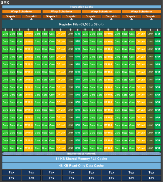
GK110 SMX
GK110 builds on that by keeping the same general design, but tweaking it for GK110’s compute-focused needs. The single biggest change here is that rather than 8 FP64 CUDA cores GK110 has 64 FP64 CUDA cores, giving it 8 times the FP64 performance of a GK104 SMX. The SMXes are otherwise very similar at a high level, featuring the same 256KB of register file space, 64KB of L1 cache, 48KB of uniform cache, and the same warp scheduler structure. This of course does not include a number of low level changes that further set apart GK104 and GK110.
Meanwhile this comparison gets much more jarring if we take a look at GK110 versus GF100 and by extension Tesla K20 versus its direct predecessors, the Fermi based Tesla family. The GK110 SMX compared to the GF100 SM is nothing short of a massive change. Superficially NVIDIA has packed many more CUDA cores into an SMX than they have an SM due to the change from a shader design that ran fewer CUDA cores at a very high (double pumped) clockspeed to a design that runs many more CUDA cores at a lower (single pumped) clockspeed, but they also have changed their warp execution model on its head in the process.

GF100/GF110 SM
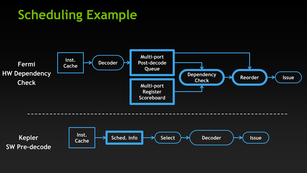
GF100 was essentially a thread level parallelism design, with each SM executing a single instruction from up to two warps. At the same time certain math instructions had variable latencies, so GF100 utilized a complex hardware scoreboard to do the necessary scheduling. Compared to that, GK110 introduces instruction level parallelism to the mix, making the GPU reliant on a mix of high TLP and high ILP to achieve maximum performance. The GPU now executes from 4 warps, ultimately executing up to 8 instructions at once if all of the warps have ILP-suitable instructions waiting. At the same time scheduling has been moved from hardware to software, with NVIDIA’s compiler now statically scheduling warps thanks to the fact that every math instruction now has a fixed latency. Finally, to further improve SMX utilization FP64 instructions can now be paired with other instructions, whereas on GF100 they had to be done on their own.
The end result is that at an execution level NVIDIA has sacrificed some of GF100’s performance consistency by introducing superscalar execution – and ultimately becoming reliant on it for maximum performance. At the same time they have introduced a new type of consistency (and removed a level of complexity) by moving to fixed latency instructions and a static scheduled compiler. Thankfully a ton of these details are abstracted from programmers and handled by NVIDIA’s compiler, but for HPC users who are used to getting their hands dirty with low level code they are going to find that GK110 is more different than it would seem at first glance.
With that said, even with the significant changes to their warp execution model, GK110 brings more changes yet. We can’t hope to replicate the sheer amount of depth NVIDIA’s own GK110 whitepaper covers, but there are several other low-level changes that further separate GK110 from GF100.
Space and bandwidth for both the register file and the L2 cache have been greatly increased for GK110. At the SMX level GK110 has 256KB of register file space, composed of 65K 32bit registers, as compared to 128KB of such space (32K registers) on GF100. Bandwidth to those register files has in turn been doubled, allowing GK110 to read from those register files faster than ever before. As for the L2 cache, it has received a very similar treatment. GK110 uses an L2 cache up to 1.5MB, twice as big as GF110; and that L2 cache bandwidth has also been doubled.
What makes this all the more interesting is that while NVIDIA significantly increased the number of CUDA cores in an SM(X), in fact by far more than the increase in cache and register file sizes, they only marginally increased the number of threads that are actually active on an SMX. Each GK110 SMX can only have up to 2K threads at any time, 1.33x that of GF100 and its 1.5K threads. So as a result GK110 is working from a thread pool only slightly larger than what GF100 worked with, which means that despite the increase in CUDA cores they actually improve their performance in register-starved scenarios as there are more registers available to each thread. This goes hand in hand with an increase in the total number of registers each thread can address, moving from 63 registers per thread on GF100 to 255 registers per thread with GK110.
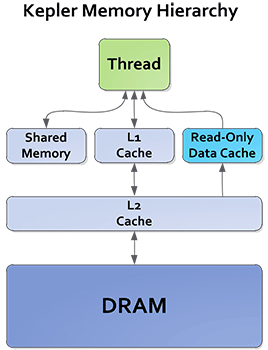
While we’re on the subject of caches, it’s also worth noting that NVIDIA has reworked their texture cache to be more useful for compute. On GF100 the 12KB texture cache was just that, a texture cache, only available to the texture units. As it turns out, clever programmers were using the texture cache as another data cache by mapping normal data at texture data, so NVIDIA has promoted the texture cache to a larger, more capable cache on GK110. Now measuring 48KB in size, in compute mode the texture cache becomes a read-only cache, specializing in unaligned memory access patterns. Furthermore error detection capabilities have been added to it to make it safer for use with workloads that rely on ECC.
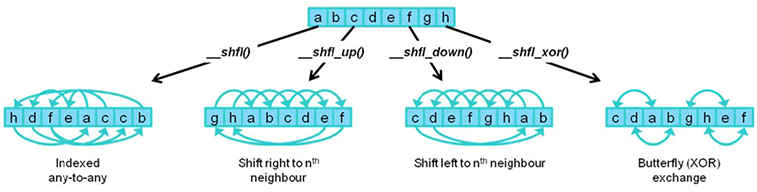
Last, but certainly not least in our low level look, NVIDIA has added a number of new instructions and operations to GK110 to further improve performance. New shuffle instructions allow for threads within a warp to share (i.e. shuffle) data without going to shared memory, making the process much faster than the old load/share/store method. Meanwhile atomic operations have also been overhauled, with NVIDIA both speeding up the execution speed of atomic operations and adding some FP64 operations that were previously only available for FP32 data.


73 Comments
View All Comments
DanNeely - Monday, November 12, 2012 - link
The Tesla (and quadro) cards have always been much more expensive than their consumer equivalents. The Fermi generation M2090 and M2070Q were priced at the same several thousand dollar pricepoint as K20 family; but the gaming oriented 570/580 were at the normal several hundred dollar prices you'd expect for a high end GPU.wiyosaya - Tuesday, November 13, 2012 - link
Yes, I understand that; however, IMHO, the performance differences are not significant enough to justify the huge price difference unless you work in very high end modeling or simulation.To me, with this generation of chips, this changes. I paid close attention to 680 reviews, and DP performance on 680 based cards is below that of the 580 - not, of course, that it matters to the average gamer. However, I highly doubt that the chips in these Teslas would not easily adapt to use as graphics cards.
While it is nVidia's right to sell these into any market they want, as I see it, the only market for these cards is the HPC market, and that is my point. It will be interesting to see if nVidia continues to be able to make a profit on these cards now that they are targeted only at the high-end market. With the extreme margins on these cards, I would be surprised if they are unable to make a good profit on them.
In other words, do they sell X amount at consumer prices, or do they sell Y amount at professional prices and which target market would be the better market for them in terms of profits? IMHO, X is likely the market where they will sell many times the amount of chips than they do in the Y market, but, for example, they can only charge 5X for the Y card. If they sell ten times the chips in X market, they will have lost profits buy targeting the Y market with these chips.
Also, nVidia is writing their own ticket on these. They are making the market. They know that they have a product that every supercomputing center will have on its must buy list. I doubt that they are dumb.
What I am saying here is that nVidia could sell these for almost any price they choose to any market. If nVidia wanted to, they could sell this into the home market at any price. It is nVidia that is making the choice of the price point. By selling the 680 at high-end enthusiast prices, they artificially push the price points of the market.
Each time a new card comes out, we expect it to be more expensive than the last generation, and, therefore, consumers perceive that as good reason to pay more for the card. This happens in the gaming market, too. It does not matter to the average gamer that the 580 outperforms the 680 in DP operations; what matters is that games run faster. Thus, the 680 becomes worth it to the gamer and the price of the hardware gets artificially pushed higher - as I see it.
IMHO, the problem with this is that nVidia may paint themselves into an elite market. Many companies have tried this, notably Compaq and currently Apple. Compaq failed, and Apple, depending on what analysts you listen to, is losing its creative edge - and with that may come the loss of its ability to charge high prices for its products. While nVidia may not fall into the "niche" market trap, as I see it, it is a pattern that looms on the horizon, and nVidia may fall into that trap if they are not careful.
CeriseCogburn - Thursday, November 29, 2012 - link
Yep, amd is dying, rumors are it's going to be bought up after a chapter bankruptcy, restructured, saved from permadeath, and of course, it's nVidia that is in danger of killing itself... LOLBoinc is that insane sound in your head.
NVidia professionals do not hear that sound, they are not insane.
shompa - Monday, November 12, 2012 - link
These are not "home computer" cards. These are cards for high performance calculations "super computers". And the prices are low for this market.The unique thing about this years launch is that Nvidia always before sold consumer cards first and supercomputer cards later. This time its the other way.
Nvidia uses the supercomputer cards for more or less subsidising its "home PC" graphic cards. Usually its the same card but with different drivers.
Home 500 dollars
Workstation 1000-1500 dollars
Supercomputing 3000+ dollars
Three different prices for the same card.
But 7 billion transistors on 28nm will be expensive for home computing. It cost more then 100% more to manufacture these GPUs then Nvidia 680.
7 BILLION. Remember that the first Pentium was the first 1 MILLION transistors. This is 7000 more dense.
kwrzesien - Monday, November 12, 2012 - link
All true.But I think what has people complaining is that this time around Nvidia isn't going to release this "big" chip to the Home market at all. They signaled this pretty clearly by putting their "middle" chip into the 680. Unless they add a new top-level part name like a 695 or something they have excluded this part from the home graphics naming scheme. Plus since it is heavily FP64 biased it may not perform well for a card that would have to be sold for ~$1000. (Remember they are already getting $500 for their middle-size chip!)
Record profits - that pretty much sums it up.
DanNeely - Monday, November 12, 2012 - link
AFAIK that was necessity speaking. The GK100 had some (unspecified) problems; forcing them to put the Gk104 in both the mid and upper range of their product line. When the rest of the GK11x series chips show up and nVidia launches the 7xx series I expect to see GK110's in the top as usual. Having seen nVidia's midrange chip trade blows with their top end one, AMD is unlikely to be resting on it's laurels for their 8xxx series.RussianSensation - Monday, November 12, 2012 - link
Great to see someone who understood the situation NV was in. Also, people think NV is a charity or something. When they were selling 2x 294mm^2 GTX690 for $1000, we can approximate that on a per wafer cost, it would have been too expensive to launch a 550-600mm^2 GK100/110 early in the year and maintain NV's expected profit margins. They also faced wafer shortages which explains why they re-allocated mobile Kepler GPUs and had to delay under $300 desktop Kepler allocation by 6+ months to fulfill 300+ notebook design wins. Sure, it's still Kepler's mid-range chip in the Kepler family, but NV had to use GK104 as flagship.CeriseCogburn - Thursday, November 29, 2012 - link
kwrsezien, another amd fanboy idiot loser with a tinfoil brain and rumor mongered brainwashed gourdEverything you said is exactly wrong.
Perhaps and OWS gathering will help your emotional turmoil, maybe you can protest in front of the nVidia campus.
Good luck, wear red.
bebimbap - Monday, November 12, 2012 - link
Each "part" being made with the "same" chip is more expensive for a reason.For example Hard drives made by the same manufacturer have different price points for enterprise, small business, and home user. I remember an Intel server rep said to use parts that are designed for their workload so enterprise "should" use an enterprise drive and so forth because of costs. And he added further that with extensive testing the bearings used in home user drives will force out their lubricant fluid causing the drive to spin slower and give read/write errors if used in certain enterprise scenarios, but if you let the drive sit on a shelf after it has "failed" it starts working perfectly again because the fluids returned to where they need to be. Enterprise drives also tend to have 1 or 2 orders of magnitude better bit read error rate than consumer drives too.
In the same way i'm sure the tesla, quadro, and gtx all have different firmwares, different accepted error rates, different loads they are tested for, and different binning. So though you say "the same card" they are different.
And home computing has changed and have gone in a different direction. No longer are we gaming in a room that needs a separate AC unit because of the 1500w of heat coming from the computer. We have moved from using 130w CPUs to only 78w. Single gpu cards are no longer using 350w but only 170w. so we went from using +600-1500w systems using ~80% efficient PSUs to using only about ~<300-600w with +90% efficient PSUs, and that is just under high loads. If we were to compare idle power, instead of only using 1/2 we are only using 1/10. We no longer need a GK110 based GPU, and it might be said that it will not make economic sense for the home user.
GK104 is good enough.
EJ257 - Monday, November 12, 2012 - link
The consumer model of this with the fully operational die will be in the $1000 range. 7 billion transitors is a really big chip even for 28nm process.