NVIDIA Launches Tesla K20 & K20X: GK110 Arrives At Last
by Ryan Smith on November 12, 2012 9:00 AM ESTContinuing our SC12 related coverage today, while AMD was the first GPU announcement of the day they are not the only one. NVIDIA is also using the venue to launch their major GPU compute product for the year: Tesla K20.
We first saw Tesla K20 at NVIDIA’s 2012 GPU Technology Conference, where NVIDIA first announced the K20 along with the already shipping K10. At the time NVIDIA was still bringing up the GPU behind K20 – GK110 – with the early announcement at GTC offering an early look at the functionality it would offer in order to prime the pump for developers. At the time we knew quite a bit about its functionality, but not its pricing, configuration, or performance.
More recently, upon completion of K20 NVIDIA has dedicated most of the initial allocation to Oak Ridge National Laboratory’s Titan supercomputer, completing delivery on a contract years in the making. As it turned out K20 was quite powerful indeed, and with K20 providing some 90% of the computational throughput of the supercomputer, Titan has taken the #1 spot on the fall Top500 supercomputer list.
This brings us to today. With Titan complete NVIDIA can now focus their attention and their GPU allocations towards making the Tesla K20 family available to the public at large. With SC12 and the announcement of the new Top500 list as their backdrop, today NVIDIA will be officially launching the Tesla K20 family of compute GPUs.
| NVIDIA Tesla Family Specification Comparison | ||||||
| Tesla K20X | Tesla K20 | Tesla M2090 | Tesla M2070Q | |||
| Stream Processors | 2688 | 2496 | 512 | 448 | ||
| Core Clock | 732MHz | 706MHz | 650MHz | 575MHz | ||
| Shader Clock | N/A | N/A | 1300MHz | 1150MHz | ||
| Memory Clock | 5.2GHz GDDR5 | 5.2GHz GDDR5 | 3.7GHz GDDR5 | 3.13GHz GDDR5 | ||
| Memory Bus Width | 384-bit | 320-bit | 384-bit | 384-bit | ||
| VRAM | 6GB | 5GB | 6GB | 6GB | ||
| Single Precision | 3.95 TFLOPS | 3.52 TFLOPS | 1.33 TFLOPS | 1.03 TFLOPS | ||
| Double Precision | 1.31 TFLOPS (1/3) | 1.17 TFLOPS (1/3) | 655 GFLOPS (1/2) | 515 GFLOPS (1/2) | ||
| Transistor Count | 7.1B | 7.1B | 3B | 3B | ||
| TDP | 235W | 225W | 250W | 225W | ||
| Manufacturing Process | TSMC 28nm | TSMC 28nm | TSMC 40nm | TSMC 40nm | ||
| Architecture | Kepler | Kepler | Fermi | Fermi | ||
| Launch Price | >$3199 | $3199? | N/A | N/A | ||
When NVIDIA first announced K20 back in May we were given a number of details about the GK110 GPU that would power it, but because they were still in the process of bringing up the final silicon for GK110 we knew little about the shipping configuration for K20. What we could say for sure is that GK110 was being built with 15 SMXes, 6 memory controllers, 1.5MB of L2 cache, and that it would offer double precision (FP64) performance that was 1/3rd its single precision (FP32 rate). Now with the launch of the K20 we finally have details on what the shipping configurations will be for K20.
First and foremost, K20 will not be a single GPU but rather it will be a family of GPUs. NVIDIA has split up what was previously announced as a single GPU into two GPUs: K20 and K20X. K20X is the more powerful of these GPUs, featuring 14 active SMXes along with all 6 memory controllers and 1.5MB of L2 cache, attached to 6GB of GDDR5. It will be clocked at 732MHz for the core clock and 5.2GHz for the memory clock. This sets a very high bar for theoretical performance, with FP32 performance at 3.95 TFLOPS, FP64 performance at 1.31 TFLOPS, and fed by some 250GB/sec of memory bandwidth. For those of you who have kept an eye on Titan, these are the same specs as the GPUs Titan, and though NVIDIA would not name it at the time we can now confirm that Titan is in fact composed of K20X GPUs and not K20.
Below K20X will be the regular K20. K20 gives up 1 SMX and 1 memory controller, giving it 13 SMXes, 5 memory controllers, 1.25MB of L2 cache, and 5GB of GDDR5. It will also be clocked slightly lower than K20X, with a shipping core clock of 706MHz while the memory clock is held at 5.2GHz. This will give K20 theoretical performance numbers around 3.52 TFLOPS for FP32, 1.17 TFLOPS for FP64, fed by 208GB/sec of memory bandwidth.
This split ends up being very similar to what NVIDIA eventually did with the Fermi generation of Tesla products such as the M2090 and M2075, spacing their products not only by performance and pricing, but also by power consumption. K20X will be NVIDIA’s leading Tesla K20 product, offering the best performance at the highest power consumption (235W). K20 meanwhile will be cheaper, a bit slower, and perhaps most importantly lower power at 225W. On that note, despite the fact that the difference is all of 10W, 225W is a very important cutoff in the HPC space – many servers and chasses are designed around that being their maximum TDP for PCIe cards – so it was important for NVIDIA to offer as fast a card as possible at this TDP, alongside the more powerful but more power hungry K20X. This tiered approach also enables the usual binning tricks, allowing NVIDIA to do something with chips that won’t hit the mark for K20X.
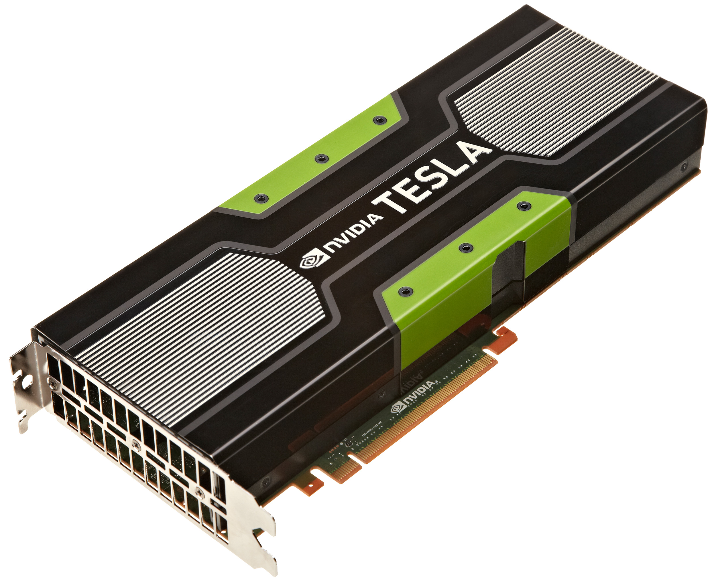
Moving on, at the moment NVIDIA is showing off the passively cooled K20 family design, confirming in the process that both K20 and K20X can be passively cooled as is the standard for servers. NVIDIA’s initial wave of focus for the Telsa K20 is going to be on servers (it is SC12 after all), but with K20 also being an integral part of NVIDIA’s next-generation Maximus strategy we’re sure to see actively cooled workstation models soon enough.


73 Comments
View All Comments
DanNeely - Monday, November 12, 2012 - link
The Tesla (and quadro) cards have always been much more expensive than their consumer equivalents. The Fermi generation M2090 and M2070Q were priced at the same several thousand dollar pricepoint as K20 family; but the gaming oriented 570/580 were at the normal several hundred dollar prices you'd expect for a high end GPU.wiyosaya - Tuesday, November 13, 2012 - link
Yes, I understand that; however, IMHO, the performance differences are not significant enough to justify the huge price difference unless you work in very high end modeling or simulation.To me, with this generation of chips, this changes. I paid close attention to 680 reviews, and DP performance on 680 based cards is below that of the 580 - not, of course, that it matters to the average gamer. However, I highly doubt that the chips in these Teslas would not easily adapt to use as graphics cards.
While it is nVidia's right to sell these into any market they want, as I see it, the only market for these cards is the HPC market, and that is my point. It will be interesting to see if nVidia continues to be able to make a profit on these cards now that they are targeted only at the high-end market. With the extreme margins on these cards, I would be surprised if they are unable to make a good profit on them.
In other words, do they sell X amount at consumer prices, or do they sell Y amount at professional prices and which target market would be the better market for them in terms of profits? IMHO, X is likely the market where they will sell many times the amount of chips than they do in the Y market, but, for example, they can only charge 5X for the Y card. If they sell ten times the chips in X market, they will have lost profits buy targeting the Y market with these chips.
Also, nVidia is writing their own ticket on these. They are making the market. They know that they have a product that every supercomputing center will have on its must buy list. I doubt that they are dumb.
What I am saying here is that nVidia could sell these for almost any price they choose to any market. If nVidia wanted to, they could sell this into the home market at any price. It is nVidia that is making the choice of the price point. By selling the 680 at high-end enthusiast prices, they artificially push the price points of the market.
Each time a new card comes out, we expect it to be more expensive than the last generation, and, therefore, consumers perceive that as good reason to pay more for the card. This happens in the gaming market, too. It does not matter to the average gamer that the 580 outperforms the 680 in DP operations; what matters is that games run faster. Thus, the 680 becomes worth it to the gamer and the price of the hardware gets artificially pushed higher - as I see it.
IMHO, the problem with this is that nVidia may paint themselves into an elite market. Many companies have tried this, notably Compaq and currently Apple. Compaq failed, and Apple, depending on what analysts you listen to, is losing its creative edge - and with that may come the loss of its ability to charge high prices for its products. While nVidia may not fall into the "niche" market trap, as I see it, it is a pattern that looms on the horizon, and nVidia may fall into that trap if they are not careful.
CeriseCogburn - Thursday, November 29, 2012 - link
Yep, amd is dying, rumors are it's going to be bought up after a chapter bankruptcy, restructured, saved from permadeath, and of course, it's nVidia that is in danger of killing itself... LOLBoinc is that insane sound in your head.
NVidia professionals do not hear that sound, they are not insane.
shompa - Monday, November 12, 2012 - link
These are not "home computer" cards. These are cards for high performance calculations "super computers". And the prices are low for this market.The unique thing about this years launch is that Nvidia always before sold consumer cards first and supercomputer cards later. This time its the other way.
Nvidia uses the supercomputer cards for more or less subsidising its "home PC" graphic cards. Usually its the same card but with different drivers.
Home 500 dollars
Workstation 1000-1500 dollars
Supercomputing 3000+ dollars
Three different prices for the same card.
But 7 billion transistors on 28nm will be expensive for home computing. It cost more then 100% more to manufacture these GPUs then Nvidia 680.
7 BILLION. Remember that the first Pentium was the first 1 MILLION transistors. This is 7000 more dense.
kwrzesien - Monday, November 12, 2012 - link
All true.But I think what has people complaining is that this time around Nvidia isn't going to release this "big" chip to the Home market at all. They signaled this pretty clearly by putting their "middle" chip into the 680. Unless they add a new top-level part name like a 695 or something they have excluded this part from the home graphics naming scheme. Plus since it is heavily FP64 biased it may not perform well for a card that would have to be sold for ~$1000. (Remember they are already getting $500 for their middle-size chip!)
Record profits - that pretty much sums it up.
DanNeely - Monday, November 12, 2012 - link
AFAIK that was necessity speaking. The GK100 had some (unspecified) problems; forcing them to put the Gk104 in both the mid and upper range of their product line. When the rest of the GK11x series chips show up and nVidia launches the 7xx series I expect to see GK110's in the top as usual. Having seen nVidia's midrange chip trade blows with their top end one, AMD is unlikely to be resting on it's laurels for their 8xxx series.RussianSensation - Monday, November 12, 2012 - link
Great to see someone who understood the situation NV was in. Also, people think NV is a charity or something. When they were selling 2x 294mm^2 GTX690 for $1000, we can approximate that on a per wafer cost, it would have been too expensive to launch a 550-600mm^2 GK100/110 early in the year and maintain NV's expected profit margins. They also faced wafer shortages which explains why they re-allocated mobile Kepler GPUs and had to delay under $300 desktop Kepler allocation by 6+ months to fulfill 300+ notebook design wins. Sure, it's still Kepler's mid-range chip in the Kepler family, but NV had to use GK104 as flagship.CeriseCogburn - Thursday, November 29, 2012 - link
kwrsezien, another amd fanboy idiot loser with a tinfoil brain and rumor mongered brainwashed gourdEverything you said is exactly wrong.
Perhaps and OWS gathering will help your emotional turmoil, maybe you can protest in front of the nVidia campus.
Good luck, wear red.
bebimbap - Monday, November 12, 2012 - link
Each "part" being made with the "same" chip is more expensive for a reason.For example Hard drives made by the same manufacturer have different price points for enterprise, small business, and home user. I remember an Intel server rep said to use parts that are designed for their workload so enterprise "should" use an enterprise drive and so forth because of costs. And he added further that with extensive testing the bearings used in home user drives will force out their lubricant fluid causing the drive to spin slower and give read/write errors if used in certain enterprise scenarios, but if you let the drive sit on a shelf after it has "failed" it starts working perfectly again because the fluids returned to where they need to be. Enterprise drives also tend to have 1 or 2 orders of magnitude better bit read error rate than consumer drives too.
In the same way i'm sure the tesla, quadro, and gtx all have different firmwares, different accepted error rates, different loads they are tested for, and different binning. So though you say "the same card" they are different.
And home computing has changed and have gone in a different direction. No longer are we gaming in a room that needs a separate AC unit because of the 1500w of heat coming from the computer. We have moved from using 130w CPUs to only 78w. Single gpu cards are no longer using 350w but only 170w. so we went from using +600-1500w systems using ~80% efficient PSUs to using only about ~<300-600w with +90% efficient PSUs, and that is just under high loads. If we were to compare idle power, instead of only using 1/2 we are only using 1/10. We no longer need a GK110 based GPU, and it might be said that it will not make economic sense for the home user.
GK104 is good enough.
EJ257 - Monday, November 12, 2012 - link
The consumer model of this with the fully operational die will be in the $1000 range. 7 billion transitors is a really big chip even for 28nm process.