The Intel SSD DC S3700: Intel's 3rd Generation Controller Analyzed
by Anand Lal Shimpi on November 5, 2012 12:01 PM EST- Posted in
- Cloud Computing
- Storage
- IT Computing
- SSDs
- Intel
A Brand New Architecture
To understand how the S3700 is different, we need to revisit how SSDs work. I've done this several times over the years so I'll keep it as succinct as possible here. SSDs are made up of a bunch of NAND packages, each with 1 - 8 NAND die per package, with each die made of multiple planes, blocks and finally pages.
NAND is solid-state, non-volatile memory (data is retained even when power is removed, courtesy of some awesome physics). There are no moving parts, and accesses are very memory-like which delivers great sequential and random IO performance. The downside is NAND has some very strict guidelines dictating how it is written to and erased.
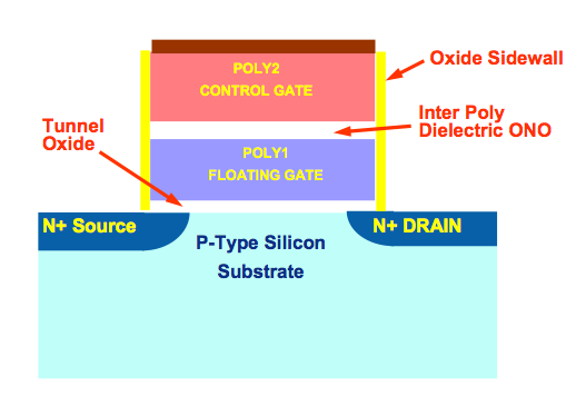
The first thing to know about NAND flash is that you can only write to the same NAND cell a finite number of times. The total amount of charge stored in a NAND cell is counted in dozens of electrons. The tunneling process that places the electrons on the floating gate (thus storing data) weakens the silicon oxide insulation layer that keeps the charge there. Over time, that layer degrades to the point where the cell can no longer store data, and it has to be marked as bad/unusable.
The second principle of dealing with NAND is that you can only write to NAND at the page level. In modern drives that's a granularity of 8KB.
The final piece of the puzzle, and the component that makes all of this a pain to deal with is that you can only erase NAND at the block level, which for Intel's 25nm NAND is 256 pages (2048KB).
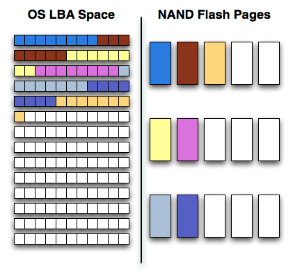
Modern SSDs present themselves just like hard drives do, as a linear array of logical block addresses. The OS sends an address and command to the SSD, and the controller translates that address to a physical location in NAND.
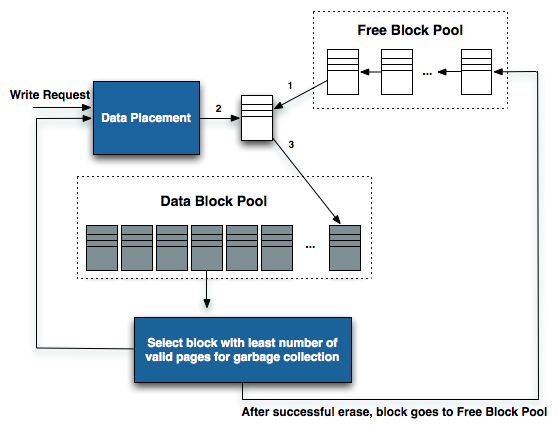
When writing to an SSD, the SSD controller must balance its desire for performance (striping writes across as many parallel NAND die as possible) with the goal of preserving NAND lifespan by writing to all cells evenly (wear leveling).
As writes come in, new pages are allocated from a pool of free blocks. As the process of erasing a NAND cell reduces endurance, a good SSD controller will prefer allocating an empty page for new data over erasing an old block. Eventually the controller will run out of clean/empty pages to write to and will have to recycle an old block filled (sometimes only partially) with invalid data to keep operating. This process can reduce overall performance and increase wear on the NAND.
When writing sequential data to an SSD it's easy to optimize for performance. Transfers can be broken up and striped across all available NAND die. Reading the data back is perfectly optimized for high performance as well. It's random IO that causes a problem for performance. Writes to random LBA locations are combined and sent out as burst traffic to look sequential, however the mapping of those LBAs to physical NAND locations can leave the drive in a very fragmented state. With enough random data fragmented on a drive, all write performance will suffer as the controller will no longer be able to quickly allocate large contiguous blocks of free pages across all NAND die.
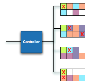
SSD in a fragmented state, white blocks represent free pages, Xes represent invalid data, colored blocks are valid data - more detail here
Modern SSD controllers will attempt to defragment themselves either while the drive is in use, or during periods of idle time (hence the phrase idle garbage collection). Adequate defragmentation is necessary to maintain a drive's performance even after it has been used for a while. The best controllers do a great job of defragmenting themselves as they work, while the worst allow internal fragmentation to get out of hand.
With that recap out of the way, let's talk about how Intel's first and second generation SSD controllers worked.
The Indirection Table
There never was a true Intel X25-M G3, the third generation controller went missing after briefly appearing on Intel roadmaps. Instead we got mild revisions of the X25-M G2's controller with new features enabled through firmware. This old controller was used in the Intel SSD 320 and more recently in the Intel SSD 710.
One notable characteristic of this old controller was that it never required a large external DRAM (16 - 64MB for the early drives). Intel was proud of the fact that it stored no user data in DRAM, which I always assumed kept the size requirements down. It turns out there was another reason.
All controllers have to map logical block addresses to physical locations in NAND. This map is stored on the NAND itself (and wear leveled so it actually moves locations), but it's cached in DRAM for fast access. Intel calls this map its indirection table.
In the old drives, the indirection table was a binary tree. A binary tree is a data structure made up of nodes and branches where each node can have at most two children.
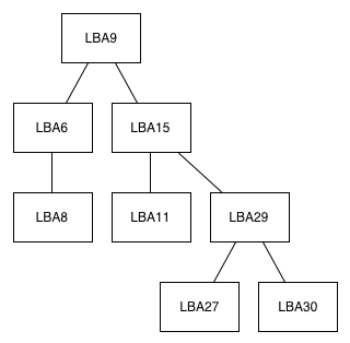
An example of an LBA-tracking binary tree, Intel's implementation is obviously far more complex. This tree can get huge.
The old indirection table grew in size as the drive was written to. Each node would keep track of a handful of data including logical block address and the physical NAND location that the block mapped to. The mapping wasn't 1:1 so many nodes would refer to a starting LBA address in addition to an offset, allowing a single node to refer to a range of physical locations.
As write requests came in, sequential data was stored as LBA + offset per node in the binary tree. Non-sequential data created a new node, growing the tree, and increasing lookup time. The tree remained balanced (for low-overhead searches, comp sci majors will remember that there's a direct relationship between the height of a binary tree and how long it takes to perform inserts/lookups on the tree), so the creation of new nodes could sometimes be very time intensive.
Given the very small DRAM that Intel wanted on its drives (to help keep costs as low as possible) and the increasing lookup times from managing an ever expanding tree, Intel would regularly defragment/compress the tree. With enough data in the tree you could actually begin compressing various nodes in the tree down into a single node. For example we might have two separate nodes in the tree that refer to sequential physical locations, which can be combined into a single node with location + offset. The tree defrag/compression process would contribute to high latency with random IO.
There was another problem however. The physical NAND had to be defragmented on a regular basis to keep pages contiguous and avoid a random sprinkling of pages on each block (this can negatively impact sequential IO performance if you go to write a large block of data and it either has to be split up amongst multiple randomly distributed blocks, or if you have to erase and rewrite a bunch of blocks to make room for the new data). The problem was that once NAND was defragmented, the logical to physical mapping tree had to be updated to reflect the new mapping, which could sometimes conflict. There could be situations where the tree could just be finished compressing itself, but the NAND would defrag itself forcing a recompression/reorganization of the tree. The fact that both the mapping tree and physical NAND had to be defragmented, and the fact that doing one could create more work for the other contributed to some potentially high latencies in the old design.
The old Intel controller had to defragment both the indirection table and the physical NAND space, and the two processes could conflict, which would create some unexpectedly high latency IO from time to time. On average, Intel was able to keep this under control, but when given the opportunity to start from scratch one major goal was to eliminate this cause of latency.


43 Comments
View All Comments
Kevin G - Monday, November 5, 2012 - link
There is mention of a large capacitor to allow for writing the cache to NAND in the event of a power failure.There are a couple of things Intel can do in this event to eliminate the possibility of cache corruption.
First is write though of any immediate change to the indirection tables. The problem of coherence between the cache and NAND would still exist but wouldn't require writing the entire cache to NAND. Making the DRAM cache write through would impact the write/erase cycles of the drive but I'm uncertain of the magnitude in comparison to heavy write IO.
The second option is that if the DRAM is used to create an optimized version of the directory tables for read only purposes, the old table in the NAND would still be valid (unless there needs to be change due to a write). Thus power loss would only lose the optimized table in DRAM but the unoptimized would still be functional in the NAND.
The third option involves optimized tables being written to disk while the unoptimized version is still in use in NAND. The last operation of writing the optimized indirection table to disk would be switching the status of what table is in active use. Thus only the optimized table is put into use after it has successfully been written to NAND. Sudden power failure in this process wouldn't impact the drive.
A fourth idea that comes to mind would be to make a reservation where the next optimized table would exist in NAND. Thus in the event of a sudden power failure, the SSD will use the unoptimized indirection tables but be able to see if anything has been written to the reserved space - it would know if it suffered a power loss and any recovery actions as necessary. This would eat space as the active table, a table being written and space for a future to be written would be 'in use'.
cdillon - Monday, November 5, 2012 - link
Personally, I don't care if an SSD stores my user data (acknowledged writes, specifically) and/or internal metadata in a DRAM cache as long as it is battery and/or capacitor backed so that cache can be flushed to NAND after a power failure.I think what I originally intended to say in my first comment was if Intel is not caching user data in DRAM, then what ARE they caching in DRAM that requires the super-capacitors to give them time to write it to NAND? If it isn't user data, then it must be the indirection tables or some other critical internal metadata. This internal metadata is at least as important as the user data itself, so why even make the distinction? The distinction stinks to me as either a marketing ploy or catering to some outdated PHB "requirement" that they need to meet in order to actually sell these drives to some enterprises. I'm not saying it's bad, just odd and probably non-optimal.
Kevin G - Monday, November 5, 2012 - link
It is likely buffering the indirection table writes to reduce the number of NAND writes. Essentially it helps with the drives overall endurance. How much so would be dependent on just how frequently the indirection table is written to.The other distinction is that they could be hitting a access time limitation by reading the indirection tables from NAND and then reading the data. By caching this in DRAM, the controller can lower access latencies to the NAND itself.
nexox - Monday, November 5, 2012 - link
Not storing user data in DRAM still helps - it forces the drive controller to actually operate efficiently instead of just fixing problems with more write cache. The indirection table doesn't change all that fast, so there won't be that much of it to flush out to NAND on power loss, but it's easy to built up a lot of user data in write cache, which requires that much more capacitance to get durably written.And FYI, many SSDs will acknowledge a write when the data hits NAND durably, but will not guarantee that the corresponding indirection table entry is durably stored, so on power failure some blocks may appear to revert to their old state, from before the synced write took place.
Death666Angel - Tuesday, November 6, 2012 - link
"Not storing user data in DRAM still helps - it forces the drive controller to actually operate efficiently instead of just fixing problems with more write cache."And why should I care how the problem is fixed?
Efficient programming or throwing more hardware at the problem is the same thing for 99% of the usage cases. If maybe power consumption is a problem, then one solution might work better than another, but for the most part, a fix is a fix, at least in my book.
Kevin G - Tuesday, November 6, 2012 - link
How the problem is fixed would matter to enterprise environments where reliability reigns supreme. How an issue is fixed in this area matters in the context of it happening again, just under different circumstances.In this example, throwing more DRAM as a write cache for SSD's would be appropriate for consumers to address the issue but not necessarily the enterprise market. Keeping data in flash maintains data integrity which matters in scenarios of sudden power failure. The thing is that enterprise markets have a different usage scenario where the large write buffer that resolved the issue for consumers could still an issue at the enterprise level (ie the SSD would need an even larger DRAM buffer).
Bullwinkle J Moose - Monday, November 5, 2012 - link
Did I miss something?With 1:1 mapping, this this sounds like the Worlds first truly O.S. agnostic controller
Does it require an O.S. with Trim or a partition offset for XP use, or did Intel just make the Worlds first universal SSD?
The 320 may have handled partition offsets internally but still required Trim for best performance
Please correct me if I'm wrong
jwilliams4200 - Tuesday, November 6, 2012 - link
You're wrong. You have misunderstood how the indirection table works.iwod - Monday, November 5, 2012 - link
The only new, and truly innovation in this controller is the actually the software side of thing. 1:1 mapping and basically super fast storage table for updating, deleting by ECC RAM.Couldn't 70 - 90% of this performance gain be implemented with other controller if they had large enough ECC DRAM?
Please correct me if I'm wrong
And what are the variation of Random I/O in other Enterprise Class SSD like Fusion IO?
MrSpadge - Tuesday, November 6, 2012 - link
To me it sounds like this change requires an entirely different controller design, or at least a checking & rethinking of major parts. Intel surely didn't tell us everything that changed, just the most important result of the changes.