Intel's Haswell Architecture Analyzed: Building a New PC and a New Intel
by Anand Lal Shimpi on October 5, 2012 2:45 AM ESTThe New Sleep States: S0ix
A bunch of PC makers got together and defined the various operating modes that ACPI PCs can be in. If everyone plays by the same rules there are no surprises, which is good for the entire ecosystem.
System level power states are denoted S0 - S5. Higher S-numbers indicate deeper levels of sleep. The table below helps define the states:
| ACPI Sleeping State Definitions | ||||
| Sleeping State | Description | |||
| S0 | Awake | |||
| S1 | Low wake latency sleeping state. No system context is lost, hardware maintains all context. | |||
| S2 | Similar to S1 but CPU and system cache context is lost | |||
| S3 | All system context is lost except system memory (CPU, cache, chipset context all lost). | |||
| S4 | Lowest power, longest wake latency supported by ACPI. Hardware platform has powered off all devices, platform context is maintained. | |||
| S5 | Similar so S4 except OS doesn't save any context, requires complete boot upon wake. | |||
S0 is an operational system, while S1/S2 are various levels of idle that are transparent to the end user. S3 is otherwise known as Suspend to RAM (STR), while S4 is commonly known as hibernate or Suspend to Disk (this one is less frequently abbreviated for some reason...).
These six sleeping states have served the PC well over the years. The addition of S3 gave us fast resume from sleep, something that's often exploited when you're on the go and need to quickly transition between using your notebook and carrying it around. The ultra mobile revolution however gave us a new requirement: the ability to transact data while in an otherwise deep sleep state.
Your smartphone and tablet both fetch emails, grab Twitter updates, receive messages and calls while in their sleep state. The prevalence of always-on wireless connectivity in these devices makes all of this easy, but the PC/smartphone/tablet convergence guarantees that if the PC doesn't adopt similar functionality it won't survive in the new world.
The solution is connected standby or active idle, a feature supported both by Haswell and Clovertrail as well as all of the currently shipping ARM based smartphones and tablets. Today, transitioning into S3 sleep is initiated by closing the lid on your notebook or telling the OS to go to sleep. In Haswell (and Clovertrail), Intel introduced a new S0ix active idle state (there are multiple active idle states, e.g. S0i1, S0i3). These states promise to deliver the same power consumption as S3 sleep, but with a quick enough wake up time to get back into full S0 should you need to do something with your device.
If these states sound familiar it's because Intel first told us about them with Moorestown:
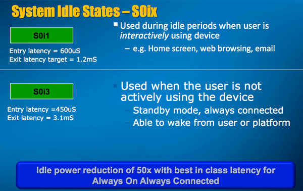
In Moorestown it takes 1ms to get out of S0i1 and only 3ms to get out of S0i3. I would expect Haswell's wakeup latencies to be similar. From the standpoint of a traditional CPU design, even 1ms is an eternity, but if you think about it from the end user perspective a 1 - 3ms wakeup delay is hardly noticeable especially when access latency is dominated by so many other factors in the chain (e.g. the network).
What specifically happens in these active idle power states? In the past Intel focused on driving power down for all of the silicon it owned: the CPU, graphics core, chipset and even WiFi. In order to make active idle a reality, Intel's reach had to extend beyond the components it makes.
With Haswell U/ULT parts, Intel will actually go in and specify recommended components for the rest of the platform. I'm talking about everything from voltage regulators to random microcontrollers on the motherboard. Even more than actual component "suggestions", Intel will also list recommended firmwares for these components. Intel gave one example where an embedded controller on a motherboard was using 30 - 50mW of power. Through some simple firmware changes Intel was able to drop this particular controller's power consumption down to 5mW. It's not rocket science, but this is Intel's way of doing some of the work that its OEM partners should have been doing for the past decade. Apple has done some of this on its own (which is why OS X based notebooks still enjoy tangibly longer idle battery life than their Windows counterparts), but Intel will be offering this to many of its key OEM partners and in a significant way.
Intel's focus on everything else in the system extends beyond power consumption - it also needs to understand the latency tolerance of everything else in the system. The shift to active idle states is a new way of thinking. In the early days of client computing there was a real focus on allowing all off-CPU controllers to work autonomously. The result of years of evolution along those lines resulted in platforms where any and everything could transact data whenever it wanted to.
By knowing how latency tolerant all of the controllers and components in the system are, hardware and OS platform power management can begin to align traffic better. Rather than everyone transacting data whenever it's ready, all of the components in the system can begin to coalesce their transfers so that the system wakes up for a short period of time to do work then quickly return to sleep. The result is a system that's more frequently asleep with bursts of lots of activity rather than frequently kept awake by small transactions. The diagram below helps illustrate the potential power savings:
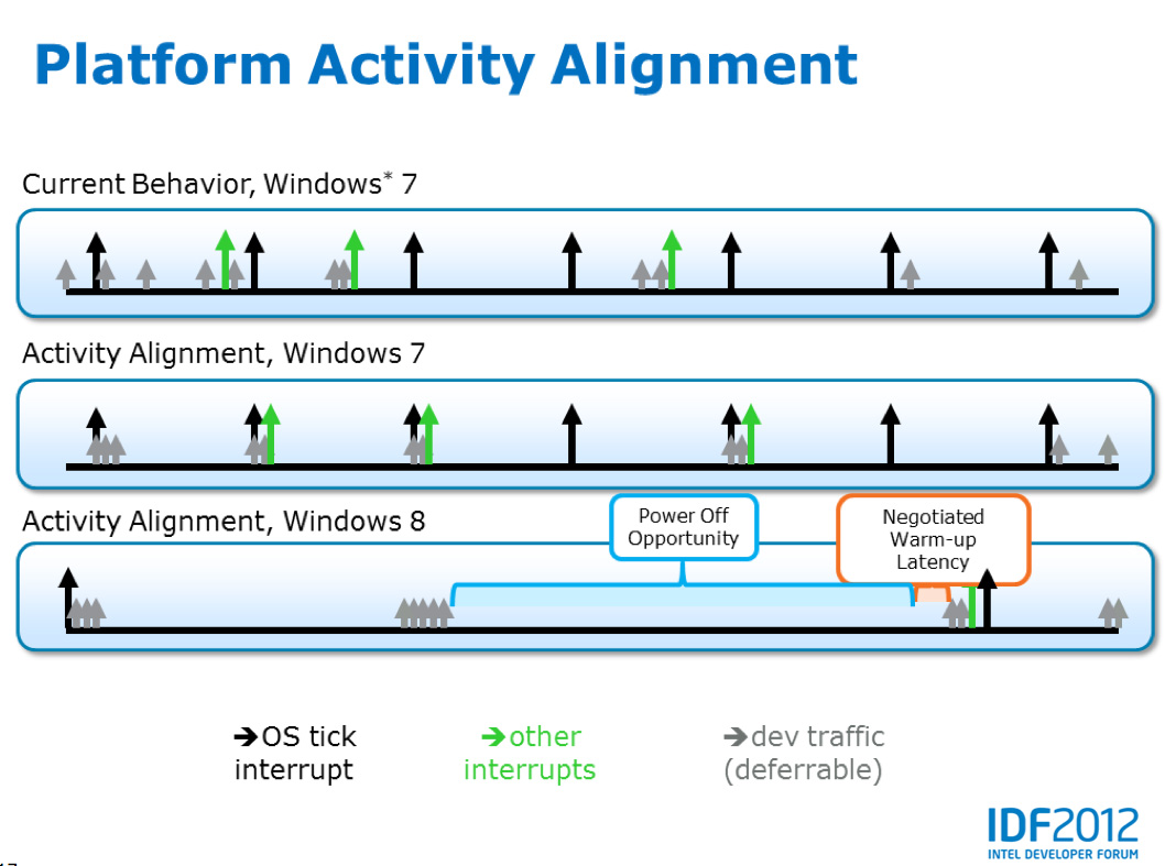
Windows 8 is pretty much a requirement to get the full benefits, although with the right drivers in place you'll see some improvement on Windows 7 as well. As most of these platform level power enhancements are targeted at 3rd generation Ultrabooks/tablets it's highly unlikely you'll see Windows 7 ship on any of them.
All of these platform level power optimizations really focus on components on the motherboard and shaving mWs here and there. There's still one major consumer of power budget that needs addressing as well: the display.
For years Intel has been talking about Panel Self Refresh (PSR) being the holy grail of improving notebook battery life. The concept is simple: even when what's on your display isn't changing (staring at text, looking at your desktop, etc...) the CPU and GPU still have to wake up to refresh the panel 60 times a second. The refresh process isn't incredibly power hungry but it's more wasteful than it needs to be given that no useful work is actually being done.
One solution is PSR. By including a little bit of DRAM on the panel itself, the display could store a copy of the frame buffer. In the event that nothing was changing on the screen, you could put the entire platform to sleep and refresh the panel by looping the same frame data stored in the panel's DRAM. The power savings would be tremendous as it'd allow your entire notebook/tablet/whatever to enter a virtual off state. You could get even more creative and start doing selective PSR where only parts of the display are updated and the rest remain in self-refresh mode (e.g. following a cursor, animating a live tile, etc...).
Display makers have been resistant to PSR because of the fact that they now have to increase their bill of materials cost by adding DRAM to the panel. The race to the bottom that we've seen in the LCD space made it unlikely that any of the panel vendors would be jumping at the opportunity to make their products more expensive. Intel believes that this time things will be different. Half of the Haswell ULT panel vendors will be enabled with Panel Self Refresh over eDP. That doesn't mean that we'll see PSR used in those machines, but it's hopefully a good indication.
Similar to what we've seen from Intel in the smartphone and tablet space, you can expect to see reference platforms built around Haswell to show OEMs exactly what they need to put down on a motherboard to deliver the sort of idle power consumption necessary to compete in the new world. It's not clear to me how Intel will enforce these guidelines, although it has a number of tools at its disposal - logo certification being the most obvious.


245 Comments
View All Comments
Da W - Friday, October 5, 2012 - link
AMD spend 1/10th of Intel in R&D. There are things they just cant do, i suspect pursuing higher x86 single trend performance is one of them.StevoLincolnite - Saturday, October 6, 2012 - link
However, allot of the R&D Intel spends is on lithography type technologies, AMD doesn't have to spend Billions on such things anymore.Besides, a simple way for AMD to beat Intel when Intel is a node ahead is to throw more transistors at the problem which they have succeeded very well at doing in the past.
Mind you, that comes at the cost of power and die size, however with stuff like clock mesh it can negate some of that.
Kevin G - Friday, October 5, 2012 - link
Being four steps behind ARM isn't necessarily a bad thing unless you're trying to leap frog them. AMD appears to be content with letting Intel spearhead the effort to get into the ultramobile market. With Intel two steps behind of ARM and they couldn't leap frog over ARM, there is little chance that AMD would be able to do the same. It isn't just knowing what battles to fight but also when to fight them.abufrejoval - Friday, October 5, 2012 - link
It was only when I was reading Jana Rutkowska's notes on the current UI limitations within Qubes, that I finally understood (I believe!) the message which AMD has been pushing for quite a few years now: GPU compute will truly be an integral part of their future APUs in one or two generations, becoming almost an augmented instruction set instead of just a SoC.Currently all Qubes "user" applications, that is everything except the Dom0, can't use the GPU to render their graphics: It's basically software rendering into an off-screen composition buffer and then GPU assisted composition of these software buffers onto the visible screen (this time with all the wobble and transition effects we've all come to expect and love ;-)
That's because although the GPU is on the same die even on the newest Trinity class APUs, it's still logically very separate, sharing only some stuff but bypassing, I believe, the ordinary page tables (not the IOMMU ones) and the snooping logic for caches. So even if GPU and CPU sit on the same die and use the same phyiscal DRAM bus, doing GPU compute implies using a dedicated part of that RAM in a way, which doesn't mesh seamlessly with CPU compute.
But the roadmap seems to imply, that this limitation will go away, which would allow e.g. Qubes to use GPU assisted rendering anywhere in user space memory and thus also into a per DomU virtual framebuffer composed of quite ordinary paged virtual memory, which could then be assembled by the Dom0 for the visible screen or for video encoding and streaming to a remote display device e.g. for cloud gaming.
This easy feeding of GPU "results" into another software layer is currently either impossible or requires major fiddling with device drivers so it's limited to the GPU vendors and bilateral deals such as nVidia and Splashtop. Once the GPU becomes more of an augmented instruction set, allowing OpenCL or even hardware primitives on ordinary user space paged virtual memory, this becomes as natural as running virtual machines with hardware virtualization.
And at that point even the new 256bit FMA may look pretty lame compared to what hundreds of APU EUs could do. That to me explains rather well, why AMD isn't spending more transistors on a vastly improved CPU only x86 ISA: It truly belives it's a dead end for both personal and scientific workloads.
It's a very daring bet and I very much admire them for having the vision and the balls to tie the company's survival to it. Over the last 40 years Intel seems to have failed with most of its visions (80432, i860, Itanium), but excelled on evolving x86. AMD, however, seems better on vision and noticably 2nd rate on execution.
APUs are potentially quite dangerous both to nVidia and to Intel, because both can't easily duplicate them: The AMD/Intel cross licensing deal IMHO won't cover the GPU portion. Unless nVidia and Intel join, which would only happen if either of the two is in truly dire straights.
But quite a few things need to fall in place over the next couple of years and AMD needs to survive them for that potential to develop. And it looks like all ther other players aren't standing still.
Events like Apple potentially using Samsung augmented cash billions to turn TMSC into a private provider of 1x nm ARM SoCs are sending shock waves into the market, which may force "strange" alliances.
These days when even trival things like "swipe to unlock" can be patented and used to bloodlet competitors I'm surprised to see IBM and Intel use things like transactional memory, which saw silocon first with Sun's Rock, I believe, or Intel turning to eDRAM for caches and frame buffers, which IBM's been implementing first on the p-Series.
That leads me to an open question on the commercial workloads, which is almost the only domain, where I have difficulties seeing the immediate benefit of APUs, at least after Oracle's grab on Java and their expressed intent to make commercial workloads a SPARC exclusive (please see Larry's opening remarks on Openworld 2012): How can AMD make APUs the better Java and database engines? How can they make search, big data, map reduced or JavaScript run better on APUs?
I can only guess that having managed CPU+GPU AMD would be in a better position to add xPU for all of the above.
ltcommanderdata - Friday, October 5, 2012 - link
A great, detailed description of Haswell's architecture. I do have some questions though.You mentioned that Intel will be including up to 1 redundant EU in the GPU array. Does that mean only GT3 will have the 1 redundant EU (41 total, 40 usable) with GT2 having no redundancy? Or is it 1 redundant EU per sub-slice, so GT2 will have 1 and GT3 will have 2?
Will the embedded DRAM be implemented PoP like in SoC? When you say we'll see a version of Haswell with embedded DRAM do will all GT3 have embedded DRAM or will only some GT3 have embedded DRAM (kind of a GT4)?
Given the long timescales of CPU design, there would be overlap between the Haifa team working on Sandy Bridge/Ivy Bridge (particularly Ivy Bridge) and the Hillsboro team working on Haswell. I was wondering if you knew how much opportunity there is for learning between consecutive designs in terms of magnitude of changes possible and timescales before things are pretty much fixed? I'm in no position to judge, but I was also wondering based on your knowledge of the architectures and/or interactions with members of the design teams if you sense any distinct difference in design philosophies between the Haifa and Hillsboro teams. Afterall, the Haifa team's background was in power-efficient, mobile-oriented designs whereas Hillsboro was high-performance, desktop/server oriented. You mentioned in the article that Haswell goes back to Nehalem's 3 clock domains due to lessons learned from Sandy Bridge/Ivy Bridge. While I don't doubt that's the primary reason, I wonder if design philosophy played a role too since Nehalem and Haswell are both Hillsboro designs and maybe they like 3 clock domains.
Anand Lal Shimpi - Friday, October 5, 2012 - link
Unfortunately that's all the info I have on redundancy in the GPU array. I think we'll have to wait until we're closer to launch to know more. The same goes for the nature of the on-package memory.I wondered the same thing about the correlation between design teams and decisions in Nehalem/Haswell, I refrained from speculating on it in the article because I didn't necessarily see any reason to doing so, but I definitely noticed the same correlation. It could just be a coincidence though. Nothing else beyond the L3 cache frequency really stood out to me as being an obvious common thread between Nehalem and Haswell though.
Take care,
Anand
ltcommanderdata - Friday, October 5, 2012 - link
Thanks again for your insights.tipoo - Friday, October 5, 2012 - link
Speaking of the EUs, is the GT3 part twice as fast as the HD4000 with or without the eDRAM cache? The article seems to imply with, but then what is the performance without it if they've doubled the EUs? Doesn't it seem more likely they doubled performance without the cache, and the cache doubles it beyond that?telephone - Friday, October 5, 2012 - link
Anand, thanks for the insights. We all enjoyed it very much and look forward to getting the real thing into your labs.To clarify some questions:
As for the design team philosophy, the Hillsboro design team continually tries to outdo the Haifa design team and vice versa. Both teams have access to the other teams' design collateral, as we co-own the tick-tock model.
Next, the reasons for the "3" clock domains are too complicated (and confidential) to go into. Since designing for "2" clock domains is much simpler, the reason is not that we enjoy pain and misery. Suffice to say, that you are missing a very big piece of the puzzle and accurate conclusions as to why this was done cannot be drawn from the information you have. And the number of clock domains is in quotes because those are not accurate anyhow.
Sincerely,
Someone from the Hillsboro Design Team
Stahn Aileron - Friday, October 5, 2012 - link
I'm curious as to whether Intel has enough interest to drive the Atom design low enough to hit ARM power level (like Medfield) and integrate an Atom core into a Core CPU design. nVidia introduced a heterogeneous CPU in their Tegra 3 SoC. (Two different ARM core types in the CPU block). From all the stuff I've seen about Intel over the past half decade, I'm pretty sure they have the resources to pull that off. They have top-notch designers and engineers with the basic tech and designs need to start R&D on that, I think.On the other hand, if they really are trying to force a Core design in Atom territory... Well, hell ya ^_~ Still, I can't really see Core hitting the sub-1W power levels they've been able to do with Atom (Medfield). I figure using an Atom core for basic S0ix functions would be a little more power efficient than using a Core design, but I'm no silicon engineer. Intel would know about that far better than me.