Intel's Haswell Architecture Analyzed: Building a New PC and a New Intel
by Anand Lal Shimpi on October 5, 2012 2:45 AM ESTFinal Words
After the show many seemed to feel like Intel short changed us at this year's IDF when it came to architecture details and disclosures. The problem is perspective. Shortly after I returned home from the show I heard an interesting comparison: Intel detailed quite a bit about an architecture that wouldn't be shipping for another 9 months, while Apple wouldn't say a thing about an SoC that was shipping in a week. That's probably an extreme comparison given that Apple has no motivation to share details about A6 (yet), but even if you compare Intel's openness at IDF to the rest of the chip makers we cover - there's a striking contrast. We'll always want more from Intel at IDF, but I do hope that we won't see a retreat as the rest of the industry seems to be ok with non-disclosure as standard practice.
There are three conclusions that have to be made when it comes to Haswell: its CPU architecture, its platform architecture and what it means for Intel's future. Two of the three look good from my perspective. The third one is not so clear.
Intel's execution has been relentless since 2006. That's over half a decade of iterating architectures, as promised, roughly once a year. Little, big, little, big, process, architecture, process, architecture, over and over again. It's a combination of great execution on the architecture side combined with great enabling by Intel's manufacturing group. Haswell will continue to carry the torch in this regard.
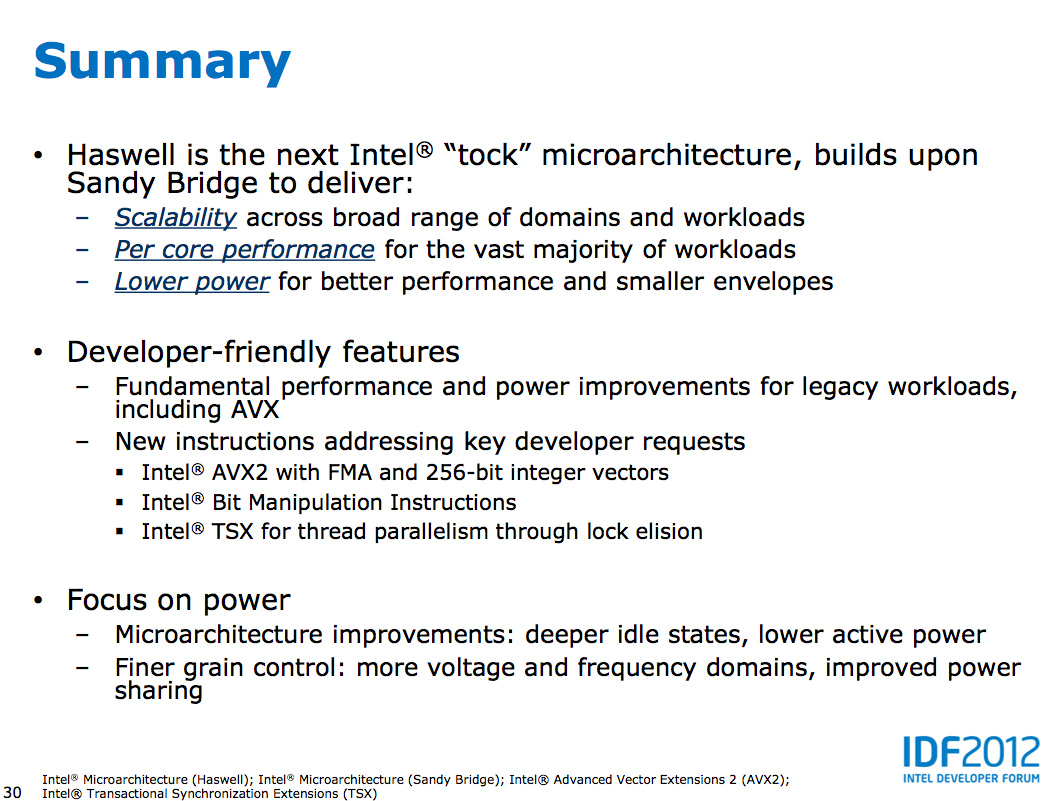
The Haswell micro-architecture focuses primarily on widening the execution engine that has been with us, moderately changed, for the past several years. Increasing data structures and buffers inside the processor helps to feed the beast, as does a tremendous increase in cache bandwidth. Support for new instructions in AVX2 via Intel's TSX should also pave the way for some big performance gains going forward. Power consumption is also a serious target for Haswell given that it must improve performance without dramatically increasing TDP. There will be slight TDP increases across the board for traditional form factors, while ultra portables will obviously shift to lower TDPs. Idle power drops while active power should obviously be higher than Ivy Bridge.
You can expect CPU performance to increase by around 5 - 15% at the same clock speed as Ivy Bridge. Graphics performance will see a far larger boost (at least in the high-end GT3 configuration) of up to 2x vs. Intel's HD 4000 in a standard voltage/TDP system. GPU performance in Ultrabooks will increase by up to 30% over HD 4000.
As a desktop or notebook microprocessor, Haswell looks very good. The architecture remains focused and delivers a sensible set of improvements over its predecessor.
As a platform, Haswell looks awesome. While the standard Haswell parts won't drive platform power down considerably, the new Haswell U/ULT parts will. Intel is promising a greater than 20x reduction in platform idle power and it's planning on delivering it by focusing its power reduction efforts beyond Intel manufactured components. Haswell Ultrabooks and tablets will have Intel's influence in many (most?) of the components placed on the motherboard. And honestly, this is something Intel (or one of its OEMs) should have done long ago. Driving down platform power is a problem that extends beyond the CPU or chipset, and it's one that requires a holistic solution. With Haswell, Intel appears committed to delivering that solution. It's not for purely altruistic reasons, but for the survival of the PC. I remember talking to Vivek about an iPad as a notebook replacement piece he was doing a while back. The biggest advantage the iPad offered over a notebook in his eyes? Battery life. Even for light workloads today's most power efficient ultraportable notebooks can't touch a good ARM based tablet. Haswell U/ULT's significant reduction in platform power is intended to fix that. I don't know that we'll get to 10+ hours of battery life on a single charge, but we should be much better off than we are today.
Connected standby is coming to PCs and it's a truly necessary addition. Haswell's support of active idle states (S0ix) is a game changer for the way portable PCs work. The bigger concern is whether or not the OEMs and ISVs will do their best to really take advantage of what Haswell offers. I know one will, but will the rest? Intel's increasingly hands on approach to OEM relations seems to be its way of ensuring we'll see Haswell live up to its potential.
Haswell, on paper, appears to do everything Intel needs to evolve the mobile PC platform. What's unclear is how far down the TDP stack Intel will be able to take the architecture. Intel seems to believe that TDPs below 8W are attainable, but it's too early to tell just how low Haswell can go. It's more than likely that Intel knows and just doesn't want to share at this point. I don't believe we'll see fanless Haswell designs, but Broadwell is another story entirely.
There's no diagram for where we go from here. Intel originally claimed that Atom would service an expanded range of TDPs all the way up to 10W. With Core architectures dipping below 10W, I do wonder if that slide was a bit of misdirection. I wonder if, instead, the real goal is to drive Core well into Atom territory. If Intel wants to solve its ARM problem, that would appear to be a very good solution.


245 Comments
View All Comments
Da W - Friday, October 5, 2012 - link
AMD spend 1/10th of Intel in R&D. There are things they just cant do, i suspect pursuing higher x86 single trend performance is one of them.StevoLincolnite - Saturday, October 6, 2012 - link
However, allot of the R&D Intel spends is on lithography type technologies, AMD doesn't have to spend Billions on such things anymore.Besides, a simple way for AMD to beat Intel when Intel is a node ahead is to throw more transistors at the problem which they have succeeded very well at doing in the past.
Mind you, that comes at the cost of power and die size, however with stuff like clock mesh it can negate some of that.
Kevin G - Friday, October 5, 2012 - link
Being four steps behind ARM isn't necessarily a bad thing unless you're trying to leap frog them. AMD appears to be content with letting Intel spearhead the effort to get into the ultramobile market. With Intel two steps behind of ARM and they couldn't leap frog over ARM, there is little chance that AMD would be able to do the same. It isn't just knowing what battles to fight but also when to fight them.abufrejoval - Friday, October 5, 2012 - link
It was only when I was reading Jana Rutkowska's notes on the current UI limitations within Qubes, that I finally understood (I believe!) the message which AMD has been pushing for quite a few years now: GPU compute will truly be an integral part of their future APUs in one or two generations, becoming almost an augmented instruction set instead of just a SoC.Currently all Qubes "user" applications, that is everything except the Dom0, can't use the GPU to render their graphics: It's basically software rendering into an off-screen composition buffer and then GPU assisted composition of these software buffers onto the visible screen (this time with all the wobble and transition effects we've all come to expect and love ;-)
That's because although the GPU is on the same die even on the newest Trinity class APUs, it's still logically very separate, sharing only some stuff but bypassing, I believe, the ordinary page tables (not the IOMMU ones) and the snooping logic for caches. So even if GPU and CPU sit on the same die and use the same phyiscal DRAM bus, doing GPU compute implies using a dedicated part of that RAM in a way, which doesn't mesh seamlessly with CPU compute.
But the roadmap seems to imply, that this limitation will go away, which would allow e.g. Qubes to use GPU assisted rendering anywhere in user space memory and thus also into a per DomU virtual framebuffer composed of quite ordinary paged virtual memory, which could then be assembled by the Dom0 for the visible screen or for video encoding and streaming to a remote display device e.g. for cloud gaming.
This easy feeding of GPU "results" into another software layer is currently either impossible or requires major fiddling with device drivers so it's limited to the GPU vendors and bilateral deals such as nVidia and Splashtop. Once the GPU becomes more of an augmented instruction set, allowing OpenCL or even hardware primitives on ordinary user space paged virtual memory, this becomes as natural as running virtual machines with hardware virtualization.
And at that point even the new 256bit FMA may look pretty lame compared to what hundreds of APU EUs could do. That to me explains rather well, why AMD isn't spending more transistors on a vastly improved CPU only x86 ISA: It truly belives it's a dead end for both personal and scientific workloads.
It's a very daring bet and I very much admire them for having the vision and the balls to tie the company's survival to it. Over the last 40 years Intel seems to have failed with most of its visions (80432, i860, Itanium), but excelled on evolving x86. AMD, however, seems better on vision and noticably 2nd rate on execution.
APUs are potentially quite dangerous both to nVidia and to Intel, because both can't easily duplicate them: The AMD/Intel cross licensing deal IMHO won't cover the GPU portion. Unless nVidia and Intel join, which would only happen if either of the two is in truly dire straights.
But quite a few things need to fall in place over the next couple of years and AMD needs to survive them for that potential to develop. And it looks like all ther other players aren't standing still.
Events like Apple potentially using Samsung augmented cash billions to turn TMSC into a private provider of 1x nm ARM SoCs are sending shock waves into the market, which may force "strange" alliances.
These days when even trival things like "swipe to unlock" can be patented and used to bloodlet competitors I'm surprised to see IBM and Intel use things like transactional memory, which saw silocon first with Sun's Rock, I believe, or Intel turning to eDRAM for caches and frame buffers, which IBM's been implementing first on the p-Series.
That leads me to an open question on the commercial workloads, which is almost the only domain, where I have difficulties seeing the immediate benefit of APUs, at least after Oracle's grab on Java and their expressed intent to make commercial workloads a SPARC exclusive (please see Larry's opening remarks on Openworld 2012): How can AMD make APUs the better Java and database engines? How can they make search, big data, map reduced or JavaScript run better on APUs?
I can only guess that having managed CPU+GPU AMD would be in a better position to add xPU for all of the above.
ltcommanderdata - Friday, October 5, 2012 - link
A great, detailed description of Haswell's architecture. I do have some questions though.You mentioned that Intel will be including up to 1 redundant EU in the GPU array. Does that mean only GT3 will have the 1 redundant EU (41 total, 40 usable) with GT2 having no redundancy? Or is it 1 redundant EU per sub-slice, so GT2 will have 1 and GT3 will have 2?
Will the embedded DRAM be implemented PoP like in SoC? When you say we'll see a version of Haswell with embedded DRAM do will all GT3 have embedded DRAM or will only some GT3 have embedded DRAM (kind of a GT4)?
Given the long timescales of CPU design, there would be overlap between the Haifa team working on Sandy Bridge/Ivy Bridge (particularly Ivy Bridge) and the Hillsboro team working on Haswell. I was wondering if you knew how much opportunity there is for learning between consecutive designs in terms of magnitude of changes possible and timescales before things are pretty much fixed? I'm in no position to judge, but I was also wondering based on your knowledge of the architectures and/or interactions with members of the design teams if you sense any distinct difference in design philosophies between the Haifa and Hillsboro teams. Afterall, the Haifa team's background was in power-efficient, mobile-oriented designs whereas Hillsboro was high-performance, desktop/server oriented. You mentioned in the article that Haswell goes back to Nehalem's 3 clock domains due to lessons learned from Sandy Bridge/Ivy Bridge. While I don't doubt that's the primary reason, I wonder if design philosophy played a role too since Nehalem and Haswell are both Hillsboro designs and maybe they like 3 clock domains.
Anand Lal Shimpi - Friday, October 5, 2012 - link
Unfortunately that's all the info I have on redundancy in the GPU array. I think we'll have to wait until we're closer to launch to know more. The same goes for the nature of the on-package memory.I wondered the same thing about the correlation between design teams and decisions in Nehalem/Haswell, I refrained from speculating on it in the article because I didn't necessarily see any reason to doing so, but I definitely noticed the same correlation. It could just be a coincidence though. Nothing else beyond the L3 cache frequency really stood out to me as being an obvious common thread between Nehalem and Haswell though.
Take care,
Anand
ltcommanderdata - Friday, October 5, 2012 - link
Thanks again for your insights.tipoo - Friday, October 5, 2012 - link
Speaking of the EUs, is the GT3 part twice as fast as the HD4000 with or without the eDRAM cache? The article seems to imply with, but then what is the performance without it if they've doubled the EUs? Doesn't it seem more likely they doubled performance without the cache, and the cache doubles it beyond that?telephone - Friday, October 5, 2012 - link
Anand, thanks for the insights. We all enjoyed it very much and look forward to getting the real thing into your labs.To clarify some questions:
As for the design team philosophy, the Hillsboro design team continually tries to outdo the Haifa design team and vice versa. Both teams have access to the other teams' design collateral, as we co-own the tick-tock model.
Next, the reasons for the "3" clock domains are too complicated (and confidential) to go into. Since designing for "2" clock domains is much simpler, the reason is not that we enjoy pain and misery. Suffice to say, that you are missing a very big piece of the puzzle and accurate conclusions as to why this was done cannot be drawn from the information you have. And the number of clock domains is in quotes because those are not accurate anyhow.
Sincerely,
Someone from the Hillsboro Design Team
Stahn Aileron - Friday, October 5, 2012 - link
I'm curious as to whether Intel has enough interest to drive the Atom design low enough to hit ARM power level (like Medfield) and integrate an Atom core into a Core CPU design. nVidia introduced a heterogeneous CPU in their Tegra 3 SoC. (Two different ARM core types in the CPU block). From all the stuff I've seen about Intel over the past half decade, I'm pretty sure they have the resources to pull that off. They have top-notch designers and engineers with the basic tech and designs need to start R&D on that, I think.On the other hand, if they really are trying to force a Core design in Atom territory... Well, hell ya ^_~ Still, I can't really see Core hitting the sub-1W power levels they've been able to do with Atom (Medfield). I figure using an Atom core for basic S0ix functions would be a little more power efficient than using a Core design, but I'm no silicon engineer. Intel would know about that far better than me.