Intel's Haswell Architecture Analyzed: Building a New PC and a New Intel
by Anand Lal Shimpi on October 5, 2012 2:45 AM ESTCPU Architecture Improvements: Background
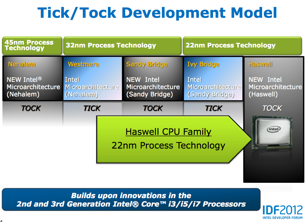
Despite all of this platform discussion, we must not forget that Haswell is the fourth tock since Intel instituted its tick-tock cadence. If you're not familiar with the terminology by now a tock is a "new" microprocessor architecture on an existing manufacturing process. In this case we're talking about Intel's 22nm 3D transistors, that first debuted with Ivy Bridge. Although Haswell is clearly SoC focused, the designs we're talking about today all use Intel's 22nm CPU process - not the 22nm SoC process that has yet to debut for Atom. It's important to not give Intel too much credit on the manufacturing front. While it has a full node advantage over the competition in the PC space, it's currently only shipping a 32nm low power SoC process. Intel may still have a more power efficient process at 32nm than its other competitors in the SoC space, but the full node advantage simply doesn't exist there yet.
Although Haswell is labeled as a new micro-architecture, it borrows heavily from those that came before it. Without going into the full details on how CPUs work I feel like we need a bit of a recap to really appreciate the changes Intel made to Haswell.
At a high level the goal of a CPU is to grab instructions from memory and execute those instructions. All of the tricks and improvements we see from one generation to the next just help to accomplish that goal faster.
The assembly line analogy for a pipelined microprocessor is over used but that's because it is quite accurate. Rather than seeing one instruction worked on at a time, modern processors feature an assembly line of steps that breaks up the grab/execute process to allow for higher throughput.
The basic pipeline is as follows: fetch, decode, execute, commit to memory. You first fetch the next instruction from memory (there's a counter and pointer that tells the CPU where to find the next instruction). You then decode that instruction into an internally understood format (this is key to enabling backwards compatibility). Next you execute the instruction (this stage, like most here, is split up into fetching data needed by the instruction among other things). Finally you commit the results of that instruction to memory and start the process over again.
Modern CPU pipelines feature many more stages than what I've outlined here. Conroe featured a 14 stage integer pipeline, Nehalem increased that to 16 stages, while Sandy Bridge saw a shift to a 14 - 19 stage pipeline (depending on hit/miss in the decoded uop cache).
The front end is responsible for fetching and decoding instructions, while the back end deals with executing them. The division between the two halves of the CPU pipeline also separates the part of the pipeline that must execute in order from the part that can execute out of order. Instructions have to be fetched and completed in program order (can't click Print until you click File first), but they can be executed in any order possible so long as the result is correct.
Why would you want to execute instructions out of order? It turns out that many instructions are either dependent on one another (e.g. C=A+B followed by E=C+D) or they need data that's not immediately available and has to be fetched from main memory (a process that can take hundreds of cycles, or an eternity in the eyes of the processor). Being able to reorder instructions before they're executed allows the processor to keep doing work rather than just sitting around waiting.
Sidebar on Performance Modeling
Microprocessor design is one giant balancing act. You model application performance and build the best architecture you can in a given die area for those applications. Tradeoffs are inevitably made as designers are bound by power, area and schedule constraints. You do the best you can this generation and try to get the low hanging fruit next time.
Performance modeling includes current applications of value, future algorithms that you expect to matter when the chip ships as well as insight from key software developers (if Apple and Microsoft tell you that they'll be doing a lot of realistic fur rendering in 4 years, you better make sure your chip is good at what they plan on doing). Obviously you can't predict everything that will happen, so you continue to model and test as new applications and workloads emerge. You feed that data back into the design loop and it continues to influence architectures down the road.
During all of this modeling, even once a design is done, you begin to notice bottlenecks in your design in various workloads. Perhaps you notice that your L1 cache is too small for some newer workloads, or that for a bunch of popular games you're seeing a memory access pattern that your prefetchers don't do a good job of predicting. More fundamentally, maybe you notice that you're decode bound more often than you'd like - or alternatively that you need more integer ALUs or FP hardware. You take this data and feed it back to the team(s) working on future architectures.
The folks working on future architectures then prioritize the wish list and work on including what they can.


245 Comments
View All Comments
random2 - Saturday, October 6, 2012 - link
"The race to the bottom that we've seen in the LCD space made it unlikely that any of the panel vendors would be jumping at the opportunity to make their products more expensive."It's unfortunate, because of what might have been had the manufacturers, of which there are only three main ones, if I recall, had the foresight to market to customers that weren't just looking to buy the lowest priced panel on display at Best Buy. Had they the initiative to have started years ago, there would be some pretty fantastic panels available today for much more reasonable prices than seen for the 27 and 30 inch 2560X1600 panels today.
Klugfan - Saturday, October 6, 2012 - link
This doesn't really belong in the Haswell article, but I would love to know more about the physics and constraints of TDP. Like, hit me with a chart of TDP impact for a variety of important parts in phones, tablets, laptops, and desktops. Show me a chart of TDP budgets and mitigation strategies. Explain to me roughly how physics forces those things to relate. Please.Seems important and it's easy to understand the comparison from Ivy Bridge to Haswell but that doesn't feel like the big picture.
havoti97 - Saturday, October 6, 2012 - link
I read the 1st page then got bored. Writing style is overly wordy... am I the only the feeling this way?xeizo - Saturday, October 6, 2012 - link
It's an article, not a twitter feed! Some of us like to get the whole picture not just the flashy stuff ....watersb - Saturday, October 6, 2012 - link
Phenomenal feature, Anand! This is why I check your site each day. Thanks very much!bill4 - Saturday, October 6, 2012 - link
like atom, you're stuck in no mans land. way too high for tablets and phones, but in desktops and laptop, who cares if the amd solution uses 30 watts instead of 8? that difference isn't enough to matter when you take the whole platform into account, especially at lower price points where battery life wont be fantastic anyway. on the dsktop it's completely pointless.JlHADJOE - Sunday, October 7, 2012 - link
On a laptop using 30 watts instead of 8 will more than triple your battery life, especially at lower price points/smaller form factors where manufacturers gimp the battery.How's about browsing for 9 hours instead of 3? Or 27 hours instead of 9? I'd jump on it in a heartbeat.
1008anan - Saturday, October 6, 2012 - link
Haswell will sport 32 single precision or 16 double precision flops per cycle per core for its desktop and high tdp mobile skews [at least 30 watt and up].Can anyone speculate on how many single precision and double precision flops per cycle per core Haswell will execute for its low TDP skews? For example the less than 10 watt skews? the 15 watt skews?
I would also be interested in learning speculation about how many execution units (or shader cores if you prefer standard nomenclature) the low TDP Haswell products will have.
1008anan - Saturday, October 6, 2012 - link
Haswell will be able to execute 16 double precision or 32 single precision flops per clock per core for desktop and high TDP mobile skews [at least 30 watts and up].Can anyone speculate on how many flops per cycle per core the sub 10 watt and 15 watt Haswell skews will execute? Similarly I would be interested in hearing speculation about how many graphic execution units (shader cores) the sub 10 watt and 15 watt Haswell products will come with. Any speculation on graphics clock speed?
Is it possible that the high end tock 22 nm Xeon server parts could have 32 double precision or 64 single precision flops per clock per core?
Laststop311 - Saturday, October 6, 2012 - link
Best explanation of haswell I've read to date. Good Job Anand.