Intel's Haswell Architecture Analyzed: Building a New PC and a New Intel
by Anand Lal Shimpi on October 5, 2012 2:45 AM ESTCPU Architecture Improvements: Background
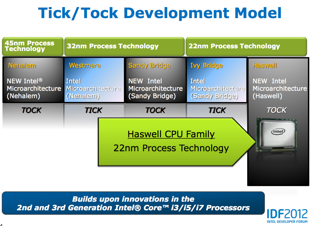
Despite all of this platform discussion, we must not forget that Haswell is the fourth tock since Intel instituted its tick-tock cadence. If you're not familiar with the terminology by now a tock is a "new" microprocessor architecture on an existing manufacturing process. In this case we're talking about Intel's 22nm 3D transistors, that first debuted with Ivy Bridge. Although Haswell is clearly SoC focused, the designs we're talking about today all use Intel's 22nm CPU process - not the 22nm SoC process that has yet to debut for Atom. It's important to not give Intel too much credit on the manufacturing front. While it has a full node advantage over the competition in the PC space, it's currently only shipping a 32nm low power SoC process. Intel may still have a more power efficient process at 32nm than its other competitors in the SoC space, but the full node advantage simply doesn't exist there yet.
Although Haswell is labeled as a new micro-architecture, it borrows heavily from those that came before it. Without going into the full details on how CPUs work I feel like we need a bit of a recap to really appreciate the changes Intel made to Haswell.
At a high level the goal of a CPU is to grab instructions from memory and execute those instructions. All of the tricks and improvements we see from one generation to the next just help to accomplish that goal faster.
The assembly line analogy for a pipelined microprocessor is over used but that's because it is quite accurate. Rather than seeing one instruction worked on at a time, modern processors feature an assembly line of steps that breaks up the grab/execute process to allow for higher throughput.
The basic pipeline is as follows: fetch, decode, execute, commit to memory. You first fetch the next instruction from memory (there's a counter and pointer that tells the CPU where to find the next instruction). You then decode that instruction into an internally understood format (this is key to enabling backwards compatibility). Next you execute the instruction (this stage, like most here, is split up into fetching data needed by the instruction among other things). Finally you commit the results of that instruction to memory and start the process over again.
Modern CPU pipelines feature many more stages than what I've outlined here. Conroe featured a 14 stage integer pipeline, Nehalem increased that to 16 stages, while Sandy Bridge saw a shift to a 14 - 19 stage pipeline (depending on hit/miss in the decoded uop cache).
The front end is responsible for fetching and decoding instructions, while the back end deals with executing them. The division between the two halves of the CPU pipeline also separates the part of the pipeline that must execute in order from the part that can execute out of order. Instructions have to be fetched and completed in program order (can't click Print until you click File first), but they can be executed in any order possible so long as the result is correct.
Why would you want to execute instructions out of order? It turns out that many instructions are either dependent on one another (e.g. C=A+B followed by E=C+D) or they need data that's not immediately available and has to be fetched from main memory (a process that can take hundreds of cycles, or an eternity in the eyes of the processor). Being able to reorder instructions before they're executed allows the processor to keep doing work rather than just sitting around waiting.
Sidebar on Performance Modeling
Microprocessor design is one giant balancing act. You model application performance and build the best architecture you can in a given die area for those applications. Tradeoffs are inevitably made as designers are bound by power, area and schedule constraints. You do the best you can this generation and try to get the low hanging fruit next time.
Performance modeling includes current applications of value, future algorithms that you expect to matter when the chip ships as well as insight from key software developers (if Apple and Microsoft tell you that they'll be doing a lot of realistic fur rendering in 4 years, you better make sure your chip is good at what they plan on doing). Obviously you can't predict everything that will happen, so you continue to model and test as new applications and workloads emerge. You feed that data back into the design loop and it continues to influence architectures down the road.
During all of this modeling, even once a design is done, you begin to notice bottlenecks in your design in various workloads. Perhaps you notice that your L1 cache is too small for some newer workloads, or that for a bunch of popular games you're seeing a memory access pattern that your prefetchers don't do a good job of predicting. More fundamentally, maybe you notice that you're decode bound more often than you'd like - or alternatively that you need more integer ALUs or FP hardware. You take this data and feed it back to the team(s) working on future architectures.
The folks working on future architectures then prioritize the wish list and work on including what they can.


245 Comments
View All Comments
kukreknecmi - Friday, October 5, 2012 - link
I hope i know it right. L3 on SB/IB doest used by GPU. L3 still servers as cache on system via memory controller. If GPU nneds to acess to memory, it sends request to memory controller. L3 is not directly accessable to GPU as a texture cache etc.On IB, they added a 512k cache which is seperated to half, 256k of it is used as texture system as backfeeding and other 256k half is used for other things.Article implies that L3 cache on IB is used as a texture buffer like on ordinary graphic cards. Only on Haswell L3 cache will be accessable and can be used as a some kind of GPU specific buffer.
Kevin G - Friday, October 5, 2012 - link
The confusing thing is that consumer Ivy Bridge parts have a L3 cache just for the GPU which is separate memory than the L3 cache that the CPU uses. The Ivy Bridge GPU's can use the CPU's L3 cache as the GPU's L4 cache to a degree.To confuse things further, the CPU side really has four levels of cache too. There is the small 1.5 KB micro-uop cache for instructions which comes before the 32 KB L1 instruction cache.
mayankleoboy1 - Friday, October 5, 2012 - link
From the article, its not very clear : Which platform (DT, Mobile, ultra mobile) will have the integrated voltage regulators/controllers ?Ryan Smith - Friday, October 5, 2012 - link
Ultra Mobile.Anand Lal Shimpi - Friday, October 5, 2012 - link
It's not clear how much of the VR circuitry gets integrated into Haswell or necessarily which parts will have it and which ones won't. Ultra mobile is a shoe in, but I've even heard of desktop parts getting it as well. We'll have to wait and see.DanNeely - Friday, October 5, 2012 - link
Rats. Reading the article I was hoping that Intel had decided to only bake the VRMs into their ultra-mobile parts. Better VRMs are an important factor in high end OCing; with desktop boards not cramped for space I really hope Intel keeps them off the package.Peanutsrevenge - Friday, October 5, 2012 - link
Seconded.However, I wonder whether the VRMs on high end mobos will still be an option, where the on package VRMs will simply extend the capabilities?
But given Intels recent distaste for overclocking, it wouldn't suprise me if we'll soon see CPUs completely locked from overclocking completely or only on E series, high profit chips.
Homeles - Saturday, October 6, 2012 - link
"However, I wonder whether the VRMs on high end mobos will still be an option, where the on package VRMs will simply extend the capabilities?"Bingo.
Homeles - Saturday, October 6, 2012 - link
Low end motherboards won't need them. High end overclocking boards will have them in addition to the ones on package.tuxRoller - Friday, October 5, 2012 - link
Using lvds reclocking you can reduce idle screen induced wakeups to 30 (ditto for the memory controller if the cpu supports self refresh for the sram ).eDP may allow even less.