The NVIDIA GeForce GTX 660 Review: GK106 Fills Out The Kepler Family
by Ryan Smith on September 13, 2012 9:00 AM ESTMeet The GeForce GTX 660
For virtual launches it’s often difficult for us to acquire reference clocked cards since NVIDIA doesn’t directly sample the press with reference cards, and today’s launch of the GeForce GTX 660 launch is one of those times. The problem stems from the fact that NVIDIA’s partners are hesitant to offer reference clocked cards to the press since they don’t want to lose to factory overclocked cards in benchmarks, which is an odd (but reasonable) concern.
For today’s launch we were able to get a reference clocked card, but in order to do so we had to agree not to show the card or name the partner who supplied the card. As it turns out this isn’t a big deal since the card we received is for all practical purposes identical to NVIDIA’s reference GTX 660, which NVIDIA has supplied pictures of. So let’s take a look at the “reference” GTX 660.
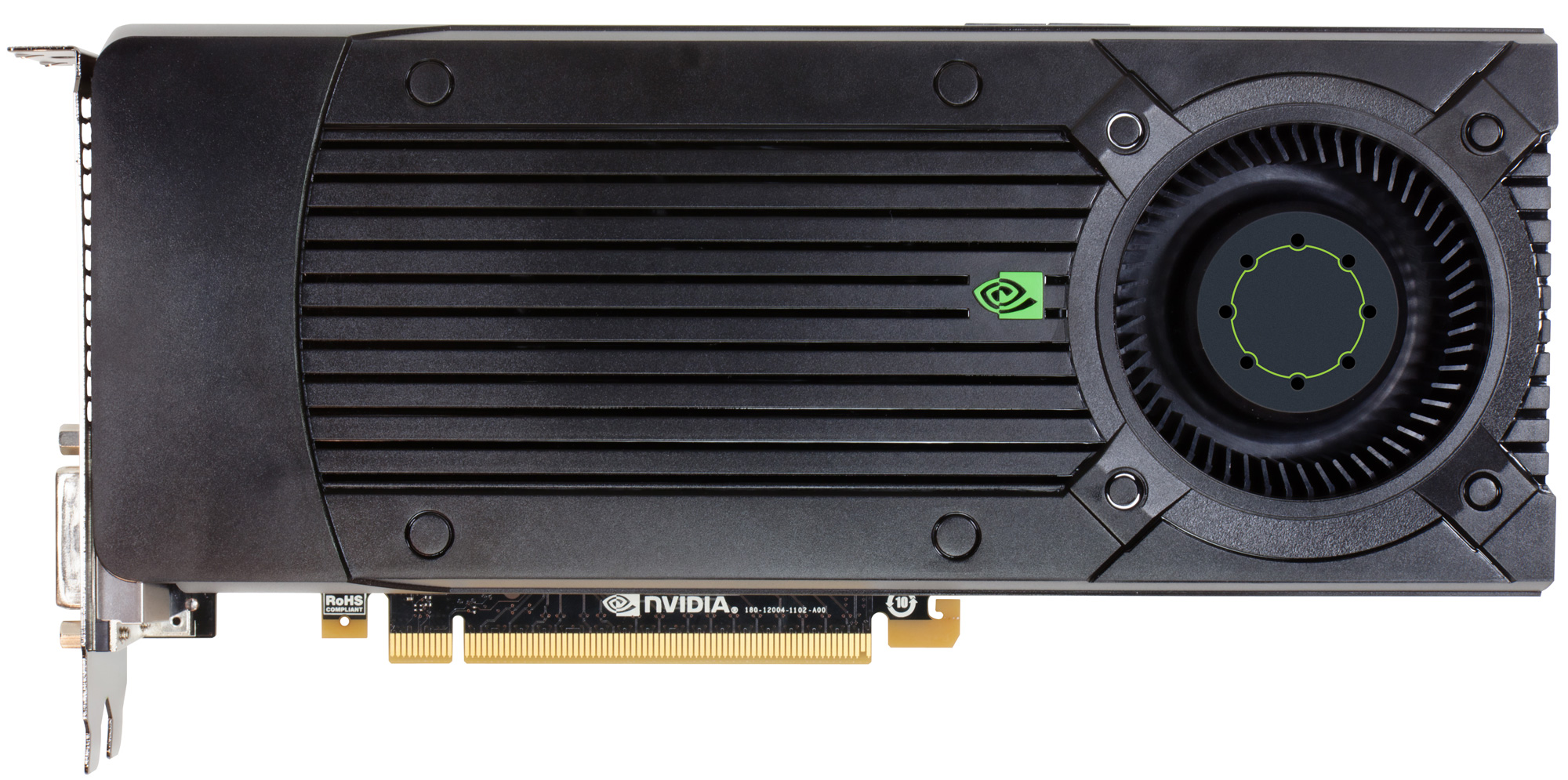
The reference GTX 660 is in many ways identical to the GTX 670, which comes as no great surprise given the similar size of their PCBs, which in turn allows NVIDIA to reuse the same cooler with little modification. Like the GTX 670, the reference GTX 660 is 9.5” long, with the PCB itself composing just 6.75” of that length while the blower and its housing composes the rest. The size of retail cards will vary between these two lengths as partners like EVGA will be implementing their own blowers similar to NVIDIA’s, while other partners like Zotac will be using open air coolers not much larger than the reference PCB itself.
Breaking open one of our factory overclocked GTX 660 (specifically, our EVGA 660 SC using the NV reference PCB), we can see that while the GTX 670 and GTX 660 are superficially similar on the outside, the PCB itself is quite different. The biggest change here is that while the 670 PCB made the unusual move of putting the VRM circuitry towards the front of the card, the GTX 660 PCB once more puts it on the far side. With the GTX 670 this was a design choice to get the GTX 670 PCB down to 6.75”, whereas with the GTX 660 it requires so little VRM circuitry in the first place that it’s no longer necessary to put that circuitry at the front of the card to find the necessary space.
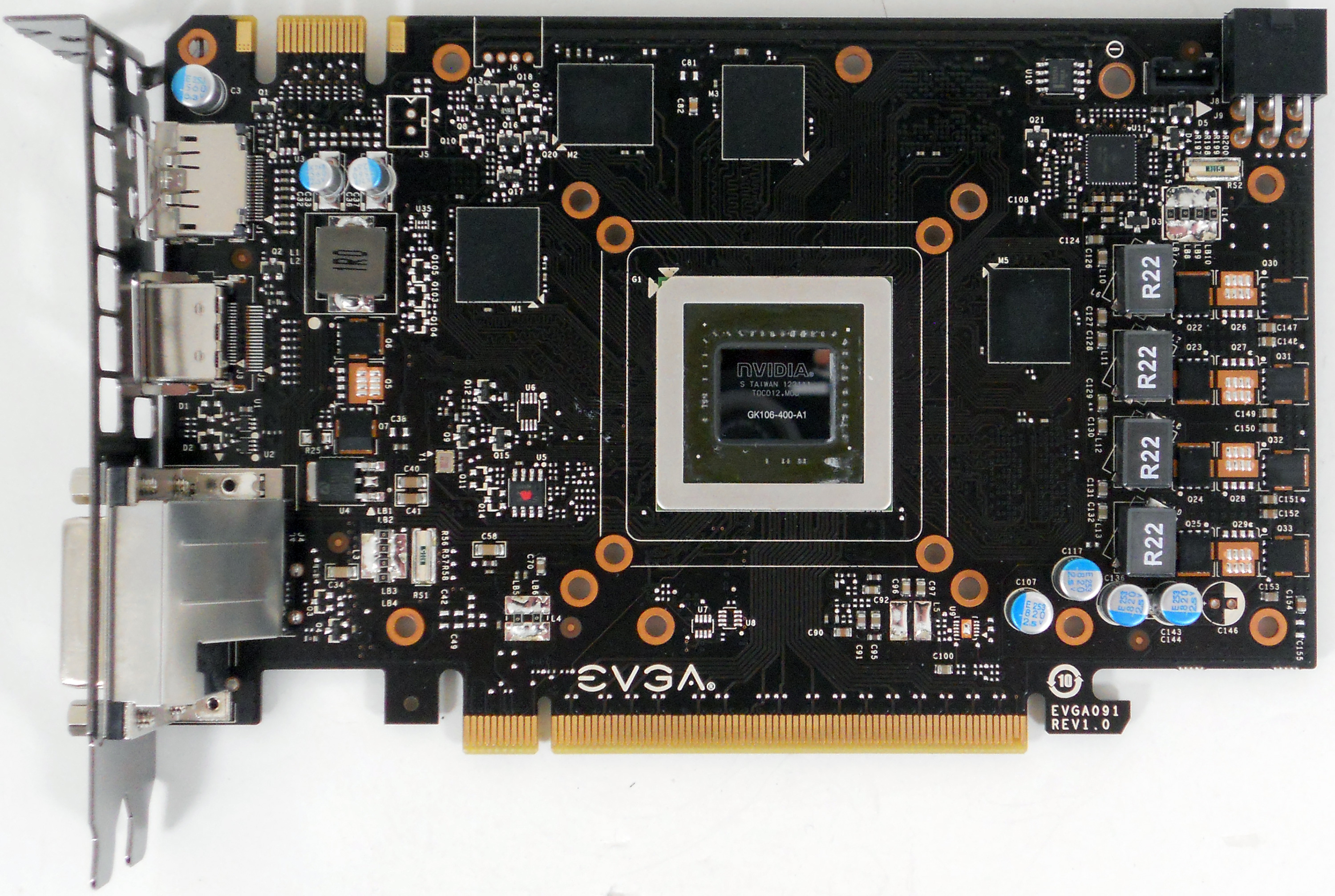
Looking at the GK106 GPU itself, we can see that not only is the GPU smaller than GK104, but the entire GPU package itself has been reduced in size. Meanwhile, not that it has any functional difference, but GK106 is a bit more rectangular than GK104.
Moving on to the GTX 660’s RAM, we find something quite interesting. Up until now NVIDIA and their partners have regularly used Hynix 6GHz GDDR5 memory modules, with that specific RAM showing up on every GTX 680, GTX 670, and GTX 660 Ti we’ve tested. The GTX 660 meanwhile is the very first card we’ve seen that’s equipped with Samsung’s 6GHz GDDR5 memory modules, marking the first time we’ve seen non-Hynix memory on a GeForce GTX 600 card. Truth be told, though it has no technical implications we’ve seen so many Hynix equipped cards from both AMD and NVIDIA that it’s refreshing to see that there is in fact more than one GDDR5 supplier in the marketplace.
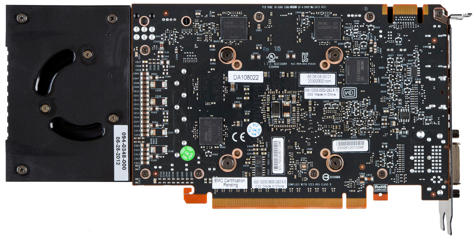
For the 2GB GTX 660, NVIDIA has outfit the card with 8 2Gb memory modules, 4 on the front and 4 on the rear. Oddly enough there aren’t any vacant RAM pads on the 2GB reference PCB, so it’s not entirely clear what partners are doing for their 3GB cards; presumably there’s a second reference PCB specifically built to house the 12 memory modules needed for 3GB cards.
Elsewhere we can find the GTX 660’s sole PCIe power socket on the rear of the card, responsible for supplying the other 75W the card needs. As for the front of the card, here we can find the card’s one SLI connector, which like previous generation mainstream video cards supports up to 2-way SLI.
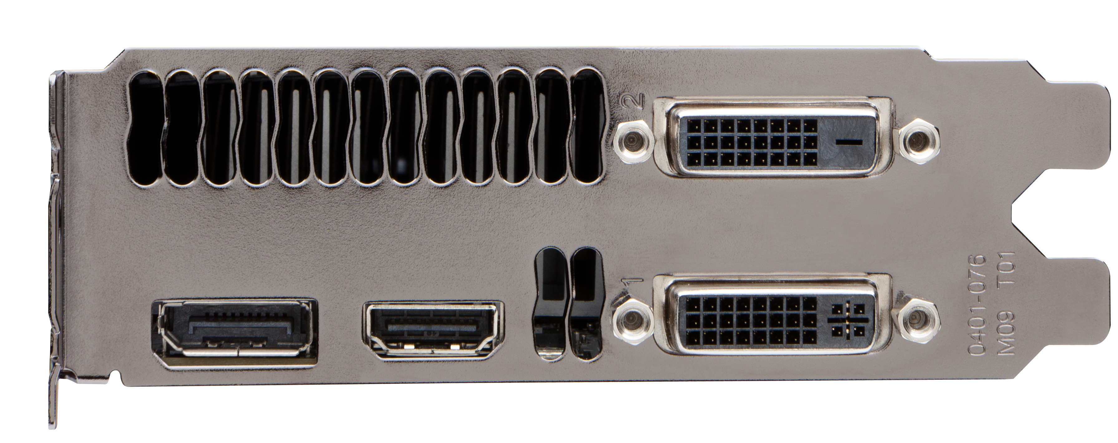
Finally, looking at display connectivity we once more see the return of NVIDIA’s standard GTX 600 series display configuration. The reference GTX 660 is equipped with 1 DL-DVI-D port, 1 DL-DVI-I port, 1 full size HDMI 1.4 port, and 1 full size DisplayPort 1.2. Like GK104 and GK107, GK106 can drive up to 4 displays, meaning all 4 ports can be put into use simultaneously.


147 Comments
View All Comments
Margalus - Thursday, September 13, 2012 - link
you say the stock 660 looks bad when compared to an overclocked 7870? what a shock that is!I guess it's always fair to say an nvidia card is bad when comparing the stock reference nv card to overclocked versions of it's nearest amd competitor..
Patflute - Friday, September 14, 2012 - link
Be fair and over clock both...poohbear - Thursday, September 13, 2012 - link
well after reading this im still have with my Gigabyte OC gtx 670 i got 2 months ago for $388. I will NOT be upgrading for 3 years & im confident my GTX 670 will still be in the upper segment in 3 years (like my 5870 that i upgraded from), so @ $130/yr its a great deal.poohbear - Thursday, September 13, 2012 - link
erm, i meant i'm still happy*. sucks that u can't edit on these comments.:pKineticHummus - Friday, September 14, 2012 - link
i had no idea what you meant with your "im still happy" edit until I went back to read your original statement again. somehow I mentally replaced the "have" with "happy" lol. reading fail for me...distinctively - Thursday, September 13, 2012 - link
Looks like the 660 is getting a nasty little spanking from the 7870 when you look around at all the reviews. The GK 106 appears to loose in just about every metric compared to Pitcairn.Locateneil - Thursday, September 13, 2012 - link
I just built a PC with 3770K and Asus Z77-v Pro, I was think to buy GTX 670 for my system but now I am now confused if it is better to go with 2 GTX 660 in SLI?Ryan Smith - Friday, September 14, 2012 - link
Our advice has always been to prefer a single more powerful card over a pair of weaker cards in SLI. SLI is a great mechanism to extend performance beyond what a single card can provide, but its inconsistent performance and inherent drawbacks (need for SLI profiles and microstuttering) means that it's not a good solution for when you can have a single, more powerful GPU.knghtwhosaysni - Thursday, September 13, 2012 - link
Do you guys think you could show frametimes like techreport does in your reviews? It can show some deficiencies in rendering that average FPS doesn't, like with Crysis 2 http://techreport.com/review/23527/nvidia-geforce-...It's nice that techreport does it, but I think Anandtech is the first stop for a lot of people who are looking for benchmarks, and I think if you guys showed this data in your own reviews then it would really push AMD and Nvidia to iron out their latency spike problems.
Ryan Smith - Friday, September 14, 2012 - link
We get asked this a lot. I really like Scott's methodology there, so if we were to do this I'd want to do more than just copy him by finding some way to do better than him (which is no easy task).To that end I find FRAPS to be at a higher level than I'd like. It's measuring when frames are handed off to the GPU rather than when the GPU actually finishes the frame. These times are strongly correlated, but I'd rather have more definitive low-level data from the GPU itself. If we could pull that off then frametimes are definitely something we'd look in to.