The GeForce GTX 660 Ti Review, Feat. EVGA, Zotac, and Gigabyte
by Ryan Smith on August 16, 2012 9:00 AM ESTThat Darn Memory Bus
Among the entire GTX 600 family, the GTX 660 Ti’s one unique feature is its memory controller layout. NVIDIA built GK104 with 4 memory controllers, each 64 bits wide, giving the entire GPU a combined memory bus width of 256 bits. These memory controllers are tied into the ROPs and L2 cache, with each controller forming part of a ROP partition containing 8 ROPs (or rather 1 ROP unit capable of processing 8 operations), 128KB of L2 cache, and the memory controller. To disable any of those things means taking out a whole ROP partition, which is exactly what NVIDIA has done.
The impact on the ROPs and the L2 cache is rather straightforward – render operation throughput is reduced by 25% and there’s 25% less L2 cache to store data in – but the loss of the memory controller is a much tougher concept to deal with. This goes for both NVIDIA on the design end and for consumers on the usage end.
256 is a nice power-of-two number. For video cards with power-of-two memory bus widths, it’s very easy to equip them with a similarly power-of-two memory capacity such as 1GB, 2GB, or 4GB of memory. For various minor technical reasons (mostly the sanity of the engineers), GPU manufacturers like sticking to power-of-two memory busses. And while this is by no means a true design constraint in video card manufacturing, there are ramifications for skipping from it.
The biggest consequence of deviating from a power-of-two memory bus is that under normal circumstances this leads to a card’s memory capacity not lining up with the bulk of the cards on the market. To use the GTX 500 series as an example, NVIDIA had 1.5GB of memory on the GTX 580 at a time when the common Radeon HD 5870 had 1GB, giving NVIDIA a 512MB advantage. Later on however the common Radeon HD 6970 had 2GB of memory, leaving NVIDIA behind by 512MB. This also had one additional consequence for NVIDIA: they needed 12 memory chips where AMD needed 8, which generally inflates the bill of materials more than the price of higher speed memory in a narrower design does. This ended up not being a problem for the GTX 580 since 1.5GB was still plenty of memory for 2010/2011 and the high pricetag could easily absorb the BoM hit, but this is not always the case.
Because NVIDIA has disabled a ROP partition on GK104 in order to make the GTX 660 Ti, they’re dropping from a power-of-two 256bit bus to an off-size 192bit bus. Under normal circumstances this means that they’d need to either reduce the amount of memory on the card from 2GB to 1.5GB, or double it to 3GB. The former is undesirable for competitive reasons (AMD has 2GB cards below the 660 Ti and 3GB cards above) not to mention the fact that 1.5GB is too small for a $300 card in 2012. The latter on the other hand incurs the BoM hit as NVIDIA moves from 8 memory chips to 12 memory chips, a scenario that the lower margin GTX 660 Ti can’t as easily absorb, not to mention how silly it would be for a GTX 680 to have less memory than a GTX 660 Ti.
Rather than take the usual route NVIDIA is going to take their own 3rd route: put 2GB of memory on the GTX 660 Ti anyhow. By putting more memory on one controller than the other two – in effect breaking the symmetry of the memory banks – NVIDIA can have 2GB of memory attached to a 192bit memory bus. This is a technique that NVIDIA has had available to them for quite some time, but it’s also something they rarely pull out and only use it when necessary.
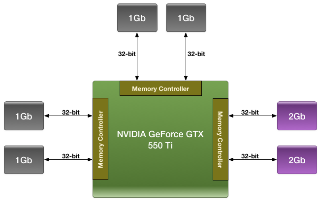
We were first introduced to this technique with the GTX 550 Ti in 2011, which had a similarly large 192bit memory bus. By using a mix of 2Gb and 1Gb modules, NVIDIA could outfit the card with 1GB of memory rather than the 1.5GB/768MB that a 192bit memory bus would typically dictate.
For the GTX 660 Ti in 2012 NVIDIA is once again going to use their asymmetrical memory technique in order to outfit the GTX 660 Ti with 2GB of memory on a 192bit bus, but they’re going to be implementing it slightly differently. Whereas the GTX 550 Ti mixed memory chip density in order to get 1GB out of 6 chips, the GTX 660 Ti will mix up the number of chips attached to each controller in order to get 2GB out of 8 chips. Specifically, there will be 4 chips instead of 2 attached to one of the memory controllers, while the other controllers will continue to have 2 chips. By doing it in this manner, this allows NVIDIA to use the same Hynix 2Gb chips they already use in the rest of the GTX 600 series, with the only high-level difference being the width of the bus connecting them.

Of course at a low-level it’s more complex than that. In a symmetrical design with an equal amount of RAM on each controller it’s rather easy to interleave memory operations across all of the controllers, which maximizes performance of the memory subsystem as a whole. However complete interleaving requires that kind of a symmetrical design, which means it’s not quite suitable for use on NVIDIA’s asymmetrical memory designs. Instead NVIDIA must start playing tricks. And when tricks are involved, there’s always a downside.
The best case scenario is always going to be that the entire 192bit bus is in use by interleaving a memory operation across all 3 controllers, giving the card 144GB/sec of memory bandwidth (192bit * 6GHz / 8). But that can only be done at up to 1.5GB of memory; the final 512MB of memory is attached to a single memory controller. This invokes the worst case scenario, where only 1 64-bit memory controller is in use and thereby reducing memory bandwidth to a much more modest 48GB/sec.
How NVIDIA spreads out memory accesses will have a great deal of impact on when we hit these scenarios. In the past we’ve tried to divine how NVIDIA is accomplishing this, but even with the compute capability of CUDA memory appears to be too far abstracted for us to test any specific theories. And because NVIDIA is continuing to label the internal details of their memory bus a competitive advantage, they’re unwilling to share the details of its operation with us. Thus we’re largely dealing with a black box here, one where poking and prodding doesn’t produce much in the way of meaningful results.
As with the GTX 550 Ti, all we can really say at this time is that the performance we get in our benchmarks is the performance we get. Our best guess remains that NVIDIA is interleaving the lower 1.5GB of address while pushing the last 512MB of address space into the larger memory bank, but we don’t have any hard data to back it up. For most users this shouldn’t be a problem (especially since GK104 is so wishy-washy at compute), but it remains that there’s always a downside to an asymmetrical memory design. With any luck one day we’ll find that downside and be able to better understand the GTX 660 Ti’s performance in the process.


313 Comments
View All Comments
badnvidia - Thursday, December 13, 2012 - link
I have purchased 2 of the new Nvidia 600 series, a gtx 660 ti, which runs fine this far, but I would question if it was worth it's cost. I purchased a second cheaper gtx 650 because cost with the promised free download of Assassins Creed III made it best choice for second computer video card. The game download promotion is a lie, tigerdirect codes are not being honored by Nvidia and I informed tigerdirect but they are still selling these cards with the promise of free game download. This is a dishonest promotion by both firms, Beware!Why support firms that are promoting these video cards with a dishonest promotion. If the free download promotion has exceeded its allotment, then both firms should stop advertising it and promising a free game download they know is not going to be honored. Shame on them for promoting such lies to customers at Christmas. I will never buy from them again.
Ajish - Sunday, March 17, 2013 - link
pls help... i have i3 2100,2 HDDs , 6 GB RAM, Corsair CX 500W psu....h61 mobo...... which one is best 660ti or 7850....both 2gb memory....m asking...... pls help.....shuko666 - Sunday, March 23, 2014 - link
mi tarjeta de video es una gtx 660 ti 1g DDR5 SE ME PONEE AL 100 % EL CONSUMO ES BUENO O MALOO? Y SE ME CALIENTA LA PC A 65 GRADOS DICEN QUE ES NORMAL PERO SE ME ME BAJAN LOS FPS EN VARIOS JUEGOS Y PUES SE SIENTE LENTA LA PC. ALGUNOS ME DICEN QUE LE PONGA UN SEIDON PARA EL CALENTAMIENTO. Y TENGO UUN PROCESADOR FX 8 3.10 3120 8GB DE RAM 1337 HZ FUENTE DE PODER 550 COOLMASTER 500 DE DISCO DURO. ALGUNA SOLUCION SERA AGRADECIDA