Samsung Announces A15/Mali-T604 Based Exynos 5 Dual
by Anand Lal Shimpi on August 10, 2012 3:04 PM EST- Posted in
- Smartphones
- Mobile
- Tablets
- SoCs
Yesterday Samsung officially announced what we all knew was coming: the Exynos 5 Dual. Due to start shipping sometime between the end of the year and early next year, the Exynos 5 Dual combines two ARM Cortex A15s with an ARM Mali-T604 GPU on a single 32nm HK+MG die from Samsung.
The CPU
Samsung's Exynos 5 Dual integrates two ARM Cortex A15 cores running at up to 1.7GHz with a shared 1MB L2 cache. The A15 is a 3-issue, Out of Order ARMv7 architecture with advanced SIMDv2 support. The memory interface side of the A15 should be much improved compared to the A9. The wider front end, beefed up internal data structures and higher clock speed will all contribute to a significant performance improvement over Cortex A9 based designs. It's even likely that we'll see A15 give Krait a run for its money, although Qualcomm is expected to introduce another revision of the Krait architecture sometime next year to improve IPC and overall performance. The A15 is also found in TI's OMAP 5. It will likely be used in NVIDIA's forthcoming Wayne SoC, as well as the Apple SoC driving the next iPad in 2013.
The Memory Interface
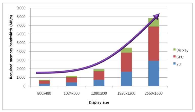
With its A5X Apple introduced the first mobile SoC with a 128-bit wide memory controller. A look at the A5X die reveals four 32-bit LPDDR2 memory partitions. The four memory channels are routed to two LPDDR2 packages each with two 32-bit interfaces (and two DRAM die) per package. Samsung, having manufactured the A5X for Apple, learned from the best. The Exynos 5 Dual is referred to as having a two-port LPDDR3-800 controller delivering 12.8GB/s of memory bandwidth. Samsung isn't specific about the width of each port, but the memory bandwidth figure tells us all we need to know. Each port is either 64-bits wide or the actual LPDDR3 data rate is 1600MHz. If I had to guess I would assume the latter. I don't know that the 32nm Exynos 5 Dual die is big eough to accommodate a 128-bit memory interface (you need to carefully balance IO pins with die size to avoid ballooning your die to accommodate a really wide interface). Either way the Exynos 5 Dual will equal Apple's A5X in terms of memory bandwidth.
TI's OMAP 5 features a 2x32-bit LPDDR2/DDR3 interface and is currently rated for data rates of up to 1066MHz, although I suspect it wouldn't be too much of a stretch to get DDR3-1600 memory working with the SoC. Qualcomm's Krait based Snapdragon S4 also has a dual-channel LPDDR2 interface, although once again there's no word on what the upper bound will be for supported memory frequencies.
The GPU
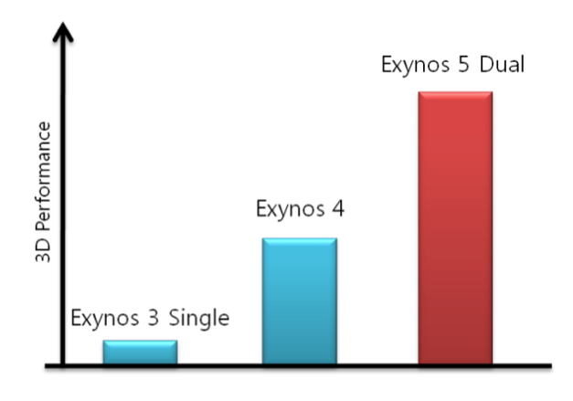
Samsung's fondness of ARM designed GPU cores continues with the Exynos 5 Dual. The ARM Mali-T604 makes its debut in the Exynos 5 Dual in quad-core form. Mali-T604 is ARM's first unified shader architecture GPU, which should help it deliver more balanced performance regardless of workload (the current Mali-400 falls short in the latest polygon heavy workloads thanks to its unbalanced pixel/vertex shader count). Each core has been improved (there are now two ALU pipes per core vs. one in the Mali-400) and core clocks should be much higher thanks to Samsung's 32nm LP process. Add in gobs of memory bandwidth and you've got a recipe for a pretty powerful GPU. Depending on clock speeds I would expect peak performance north of the PowerVR SGX 543MP2, although I'm not sure if we'll see performance greater than the 543MP4. The Mali-T604 also brings expanded API support including DirectX 11 (feature level 9_3 though, not 11_0).
Video encode and decode are rated at 1080p60.
The Rest
To complete the package Samsung integrates USB 3.0, SATA 3, HDMI 1.4 and eDP interfaces into the Exynos 5 Dual. The latter supports display resolutions up to 2560 x 1600. The complete package is the new face of a modern day mobile system on a chip.
Samsung remains very aggressive on the SoC front. The real trick will be whether or not Samsung can convince other smartphone and tablet vendors (not just Samsung Mobile) to use its solution instead of something from TI, NVIDIA or Qualcomm. As long as Samsung Mobile ships successful devices the Samsung Semiconductor folks don't have to worry too much about growing marketshare, but long term it has to be a concern.


36 Comments
View All Comments
vasanthakumar - Saturday, August 11, 2012 - link
Samsung processor is lesser power efficient when compared to APPLE. I think SAMSUNG manufactres Ax chip and it is not designing.Apple provides GDSII netlist kind of stuff to Samsung.
Dont jump into conclusion of Samsung designing APPLE chipsets. It is wrong assertion.
Death666Angel - Saturday, August 11, 2012 - link
Can you show me the evidence you base that assumption upon? Because as I see it, we can test Samsung chips in an Android environment vs Apple chips in an iOS environment which says nothing about an Android vs. iOS or the Samsung vs. Apple question you are tackling. It just says something about the Android+Samsung vs. Apple+iOS questions which this isn't about.Penti - Monday, August 13, 2012 - link
All the cell libraries are fab specific and optimized thus an ARM-core from ARM is not built for Samsung directly without work and collaboration by Samsung, the tools are for the Samsung process and so on, Samsung has their own IP for that. That they collaborate with and develop for ARM. They have their own process, they have their own transistor type/design. Any IP core will have some work by Samsung in it. Plus the netlist comes from ARM if you build with hard macro cores. Either way they are not designing the processor itself. Apple probably only has a physical IP license or uses Samsungs RTL designs. They necessarily don't generate and synthesis their own netlist (for the ARM cores) for the fab. Thus the stuff ARM and Samsung (itself a RTL licensee) cook up together or what Samsung develops from the soft cores (RTL) is likely what Apple and other customers uses. By using Samsungs stuff in their design and engineering tools. Inevitably technology from Samsung will be there even if it where an design by their own from the ground up. An design for another fab, using other tools, processes, design kits, cell libraries etc just wouldn't work. Although some companies collaborate with each other so that you can move designs more easily, that doesn't mean it's compatible with TSMC though.Regarding power, we just don't know they are two different designs sitting in different products. Samsung Semi is a design foundry. Apple also uses their packing technology (PoP) thats why you see Samsung chips on there right in the packing of the SoC.
vasanthakumar - Wednesday, August 15, 2012 - link
Correct. Cell libraries are fab specific as well as process geometries specific. Samsung advertises itself will make 32nmHK proces which is already used in sandy bridge .But I believe 20 nm and 14 nm FinFET may offer great advantages.
But some guys argue planar architecture may be greater good.(ST).
FinFET 4 terminal device has got triagular structure (Not a rectangular one) for larger yield.
ARM gives RTL code some are soft and some may be GTECH ( Un optimized gatelevel netlist).ARM is used to license architecture. Some guys like QUALCOMM optimize the RTL code for power consumption. I think Apple may also do that. Samsung has their own fab. I think for economy reasons APPLE go for Samsung. Remember a company called Portal player who designed first APPLE chips later APPLE went to Samsung for the economy. ( They offer SOC + DRAM ) combo cheaper.
Later Portal player took over by nVIDIA , nVIDIA started shipping (Tegra chipsets). Hmmm.. the disucssion is going on different direction.
Power there are two components ( they are many).... Let me explain.. Static and Dynamic... Static when transistors go in idle... Smaller geometries offer larger leakage..
Dynamic when it is powered CV2F... Usually clock gating and Multi Vt librarires are used... But High Vt cells offer greater delay and lesser leakage. There are many more schemes available for discussion sake we need have to go.
Power gating offers good power saving .. Nothing but switching off power when not used . Basically for that we need multi rails (voltages), isolation cells, retention cell ( Low power architecure).
But the devil lies in DFT.. How do we test the POwer gating .. If it fails what will happen...
Beyond that Macrocells like hardcores like RAMS, PLLs, PADS also consumes lot of power. The bad guys are PLLs and Termination.
They consume lot of power.
If you enlighten me with more info , I am ready to hear...
Exophase - Thursday, August 16, 2012 - link
This would usually be the case, but it's well known that Intrinsity performed the design work for Samsung's Cortex-A8 Hummingbird offering on their 45nm process, and Apple bought Intrinsity.My guess is that Intrinsity licensed their hardened cores to Samsung, to make available to third parties. Now that Apple owns Intrinsity they don't have to pay that licensing fee, but maybe they're still licensing hardened Cortex-A9 and Cortex-A15 cores to Samsung for use in their own SoCs on their fabs (or maybe Samsung is doing their own versions now). In the future when Apple does their own ARM cores using PASemi's uarch design talent then chances are Intrinsity will harden those too and probably won't license it out to anyone else.
vasanthakumar - Saturday, August 18, 2012 - link
With reference to DAC 2012 conference, Wide IO is going to implemented in Samsung next processor. .But It seems it is going to be Non JEDEC Wide I/O. Samsung already claimed TSV and PDK proved in 32nm node.But the yield for Wide I/O.....
I don't believe it is going to DDR3-L(1.35) as their for Exynos 5. Misleading block diagram.
There are chances of LPDDR3..