GTC 2012 Part 1: NVIDIA Announces GK104 Based Tesla K10, GK110 Based Tesla K20
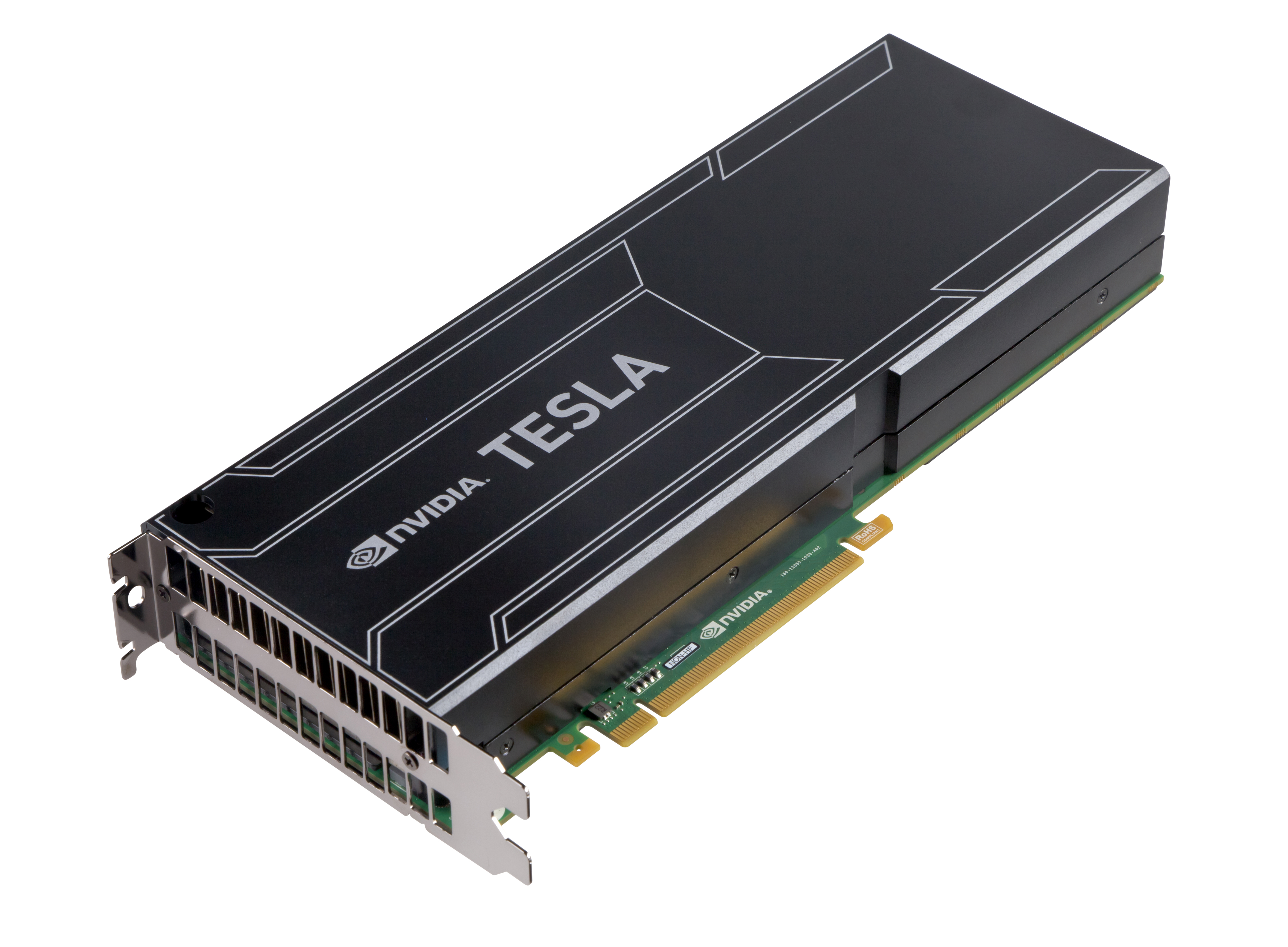
by Ryan Smith on May 17, 2012 3:15 AM ESTWe’re here at NVIDIA’s GPU Technology Conference (GTC) 2012, where NVIDIA is holding their semi-annual professional developers conference. There’s been a great deal announced that will take a few days to completely go over, but for now we wanted to start on the product side with NVIDIA’s major product announcements. With the launch of GK104 back in March NVIDIA is now ready to start rolling out some of their professional productions, and while the next generation of Quadro is not yet ready, Tesla is another matter. This brings us to our first part of our GTC coverage: the next generation of Tesla cards, Tesla K10 and Tesla K20.
| Tesla K20* | Tesla K10 | Tesla M2090 | |
| Stream Processors | <=2880 | 2 x 1536 | 512 |
| Texture Units | <=240 | 2 x 128 | 64 |
| ROPs | <=48 | 2 x 32 | 48 |
| Core Clock | ? | 745MHz | 650MHz |
| Shader Clock | N/A | N/A | 1300MHz |
| Memory Clock | ? | 5GHz GDDR5 | 3.7GHz GDDR5 |
| Memory Bus Width | 384-bit | 2 x 256-bit | 384-bit |
| L2 Cache | <=1.5MB | 2 x 512KB | 768KB |
| VRAM | ? | 2 x 4GB | 6GB |
| ECC | Full | Partial (DRAM) | Full |
| FP64 | 1/3 FP32 | 1/24 FP32 | 1/2 FP32 |
| TDP | ? | 225W | 225W |
| Transistor Count | 7.1B | 2 x 3.5B | 3B |
| Manufacturing Process | TSMC 28nm | TSMC 28nm | TSMC 40nm |
The first of the new Teslas, and the only model slated to be available in the near future is the Tesla K10. In an interesting turn of events, Tesla K10 will be based on GK104. Specifically it’s a dual-GPU card based on NVIDIA’s recently launched GTX 690, modified to fit the needs of the GPU compute market. Previous generation Tesla cards have always been based on NVIDIA’s top-tier GPUs – GT200 and GF100/GF110 respectively – so this is the first time NVIDIA has ever split the Tesla market in this way by using a lower tier GPU.
The fact of the matter is that with GK104 first launching in GeForce products, NVIDIA downplayed GK104’s compute capabilities. And our own benchmarking has established that GTX 680’s compute performance is anywhere between slightly ahead of the Fermi based GTX 580 to well behind it. Being a descendant of GF114, GK104 had a fair bit of its compute capabilities stripped out relative to GF110, not the least of which is double-precision floating point performance, ECC cache protection, and a about half of the number of registers per CUDA core relative to Fermi.
Given the questionable compute performance of GK104, this makes NVIDIA’s decision to launch a Tesla part based on it quite unexpected. Still, this is not to say that GK104 can’t perform well in the right situations and this is exactly what NVIDIA designing K10 around. The fact that we’ve found GK104 cards to be slow at compute workloads at times is not lost on NVIDIA; they know better than anyone else what GK104 really can and can’t do and have planned accordingly. For that reason NVIDIA is breaking from what little tradition there is with Tesla as a broad market product and pitching K10 at a very specific market.

NVIDIA’s market strategy here is actually summed up rather well in their K10 press release: “NVIDIA Tesla K10 GPU Accelerates Search for Oil and Gas Reserves, Signal and Image Processing for Defense Industry.” GK104 lacks the ECC and compute flexibility of the Fermi Tesla cards, but what it doesn’t lack is single-precision compute performance and memory bandwidth; and with a dual-GPU card in particular it has both of those in spades. Accordingly, NVIDIA’s goal for K10 is to go after the specific market segments that don’t need ECC and don’t need flexibility, but do need all the raw compute performance they can get. This as it turns out is something gamers are already familiar with: image processing. Image processing doesn’t need the incredible levels of precision that pure computational work does and for that matter it’s rather tolerant of the errant error, so NVIDIA believes there’s a suitably large market there that can be served by GK104 rather than GK110.
With that said, I must admit that if GK110 had come first I don’t know if we’d be having this conversation. Even if a dual GK104 card is faster splitting their market like this is not an easy to move to make. But with GK110 not due in retail for another 5-6 months it’s obviously NVIDIA’s only choice if they want to get new Tesla cards out on the market before the end of the year.
In any case we’ll know more about the full performance of K10 soon enough. Based on GTX 680 I think we already have a good idea of GK104’s basic strengths and weaknesses, but I also have to consider the possibility that NVIDIA has been sandbagging the GTX 600 series’ compute performance. NVIDIA has handicapped GeForce performance in a few different ways for quite a number of years in order to create distinct market segments, first for Quadro and more recently for Tesla. With GTX 580 this was done by handicapping both double-precision and geometry performance, but because GK104 is inherently weak at double-precision NVIDIA would need to handicap the GTX 600 series in some other manner if they wanted to maintain this kind of market segmentation. So perhaps GK104 is actually faster at compute than what we’ve seen so far?
Wrapping things up, while NVIDIA hasn’t posted every last spec for K10 they have posted enough for us to work with. Like GTX 690 K10 is using fully enabled GK104 GPUs, so based on NVIDIA’s theoretical performance data of 4.58TFLOPs with 320GB/sec of bandwidth it’s almost certainly clocked at around 745MHz core and 5GHz memory. Meanwhile for memory the card has 8GB of GDDR5, which breaks down to 16 2Gb GDDR5 modules per GPU for a total of 32 on the card. TDP is said to be identical to M2090, which would make it a 225W part. Finally, as far as availability and pricing is concerned officially K10 is available “now” though in practice partners won’t be shipping cards and systems until closer to the end of the month. Pricing is expected to be close to that of the M2090 it replaces, which would mean we’re looking at $2500 and higher.


51 Comments
View All Comments
Malphas - Thursday, May 17, 2012 - link
They'll most likely just release them as the 700 series at the tail end of this year.Musafir_86 - Thursday, May 17, 2012 - link
-They directly go with GK110? Where's GK100? Shouldn't it be released first as with Fermi (GF100 -> GF110)?Regards.
gplnpsb - Thursday, May 17, 2012 - link
Presumably there was a GK100 design that was cancelled for whatever reason. If it ever taped out (presumably around late summer of last year, around the same time as the GK104 tape out), nVidia may have realized it would be unmanufacturable on TSMCs 28nm process as it was.Rumor has it that GK110 taped out in January of this year. Perhaps nVidia had to go back and optimize the chip for yields and clock speeds once they got enough experience with the idiosyncrasies of the 28nm process.
tipoo - Thursday, May 17, 2012 - link
From Nvidias own website, it seems like these cards are far weaker than Fermi at DP operations, even with two chips it doesn't match the single chip older Fermi oneshttp://www.nvidia.com/object/tesla-servers.html
190 Gigaflops for the K10 with two GPUs, 665 and 515 for the older Fermi cards. Hmm. I thought only the consumer Geforce versions would have such cut down compute performance, but I guess it's inherent in the architecture.
Ryan Smith - Thursday, May 17, 2012 - link
To be precise, it's GK104 that has weak DP (1/24). GK110 is much better, it's 1/3, which is actually a bit lower than GF110 which was 1/2.tipoo - Thursday, May 17, 2012 - link
So the full (gk110) part would be around 1500Gflops DP if it's 1/3, or is there more to it than that?tipoo - Thursday, May 17, 2012 - link
Wait nevermind, that would be if it performed the same as the dual chip 104 which it probably won't. Do we have any idea what the DP performance of GK110 would be like then?tipoo - Thursday, May 17, 2012 - link
We need an edit button just for me, heh. Nvidias slide says the k10 is 3x the single precision performance as todays cards, the k20 is 3x the DP. So 1500Gflops is pretty close, and the rumours say 1.5Tflops too so that's a good bet I guess.Ryan Smith - Thursday, May 17, 2012 - link
NVIDIA's official guideance is >1TFLOP real performance, which is a combination of the increased number of functional units and increased efficiency on GK110.PsiAmp - Saturday, May 19, 2012 - link
If GK110 has the same clocks as GK104 then it is ~1.43 TFLOPS DP. Nvidia stated that it has ~1 TFLOPS DP performance. They can't know it yet, because chip is too far for mass production state.