NVIDIA GeForce GTX 680 Review: Retaking The Performance Crown
by Ryan Smith on March 22, 2012 9:00 AM ESTMeet the GeForce GTX 680
All things considered the design of the GeForce GTX 680 is not a radical departure from the GTX 580, but at the same time it also has some distinct differences owing to the fact that its TDP is some 50W lower than GTX 580.
Like the past GTX x80 cards, the basic design of the GTX 680 is that of a blower. A radial fan at the rear of the card sucks in air and pushes it towards the front of the card. Notably, due to a combination of card length and the fan position, the “wedge” around the fan has been done away with. NVIDIA tells us that this shouldn’t significantly impact the cooling of the card, particularly since it has a lower TDP in the first place, but when used in SLI it will remove some of the breathing room than the GTX 580 enjoyed.
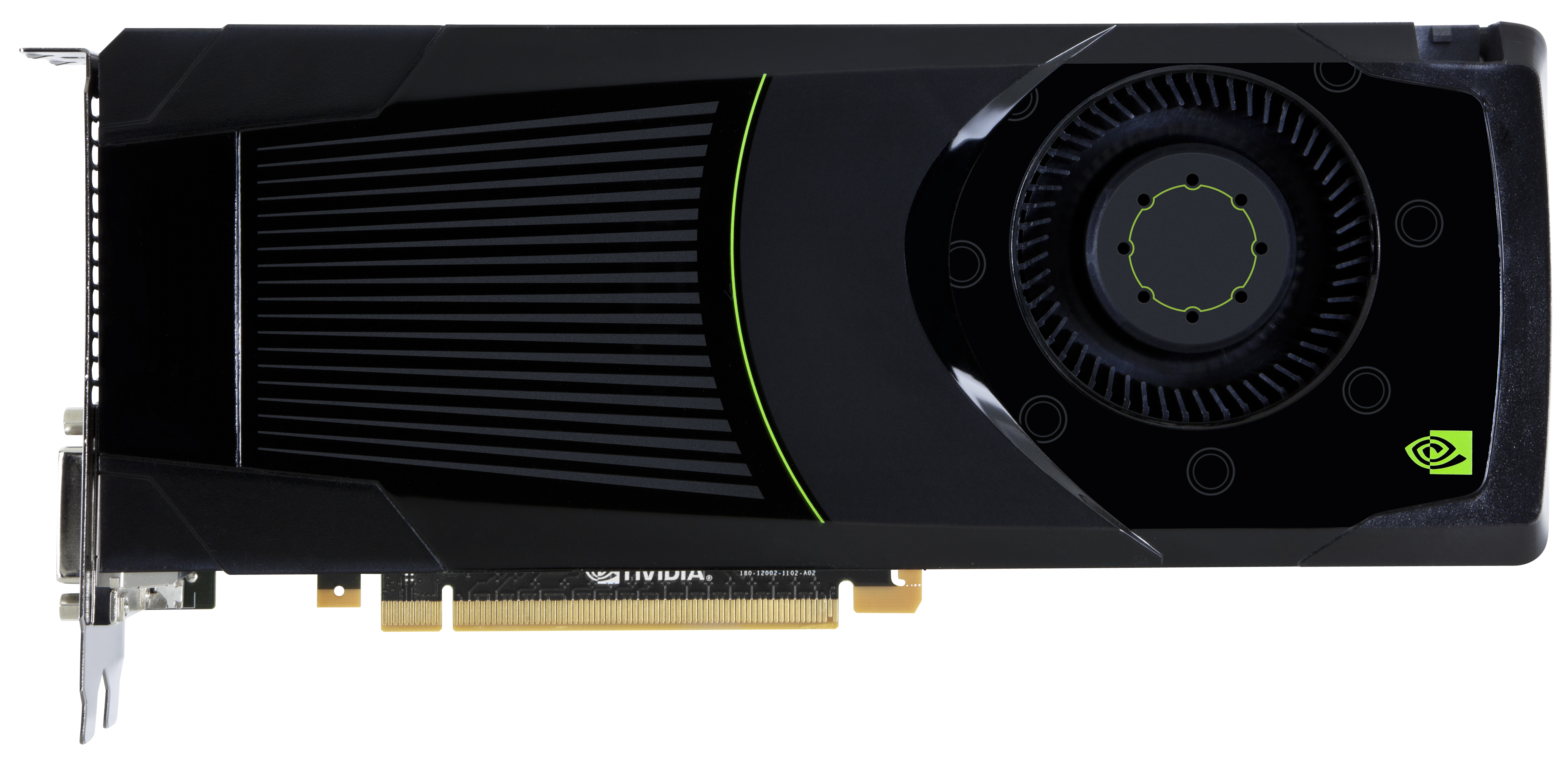
Looking at the fan itself, compared to the GTX 580 the fan has been moved from the center of the card to the top of the card. This is due to NVIDIA’s port configuration, which uses a stacked DVI connector that consumes what would have normally been part of the exhaust vent on the GTX 580. We’ll get into the port configuration more in a minute, but for the moment the significance is that because the GTX 680 only has half a vent NVIDIA has moved the fan to match the vent, which is why the fan has been moved up.
On that note, the repositioning of the fan also had its own ramifications. Because the fan is now so close to the top and at the same time so close to the rear, NVIDIA went with a unique method of arranging the PCIe power sockets. Rather than having them side-by-side as we’ve seen on countless NVIDIA cards in the past, the sockets are stacked on each other in a staggered configuration. With the fan otherwise occupying the space that one of the sockets would take up, this configuration allowed NVIDIA to have two sockets without lengthening the card just to fit another socket. Overall this staggered design is not too difficult to work with, though with one socket facing the opposite way it might require some cable repositioning if you have a well maintained cable run.
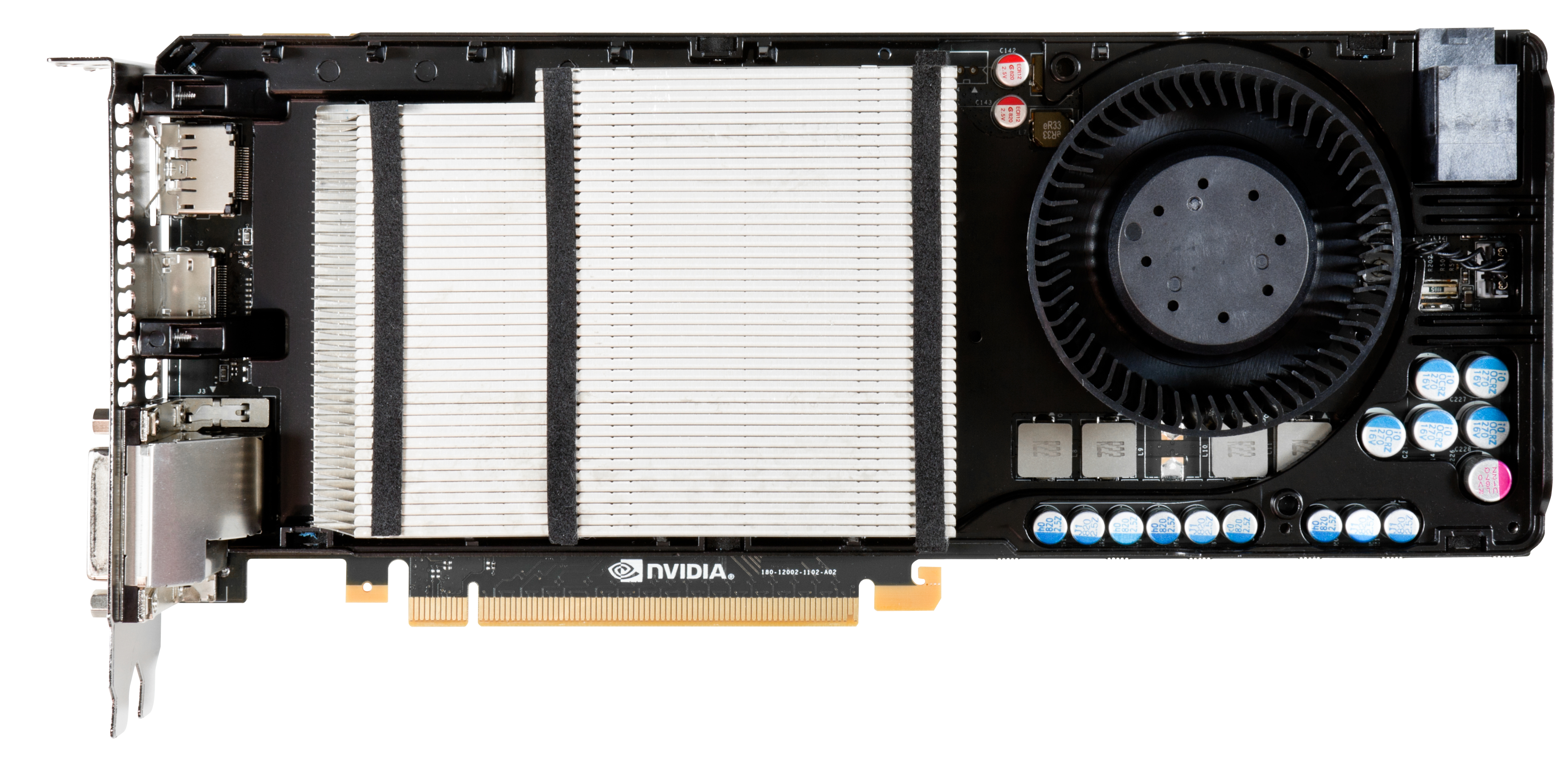
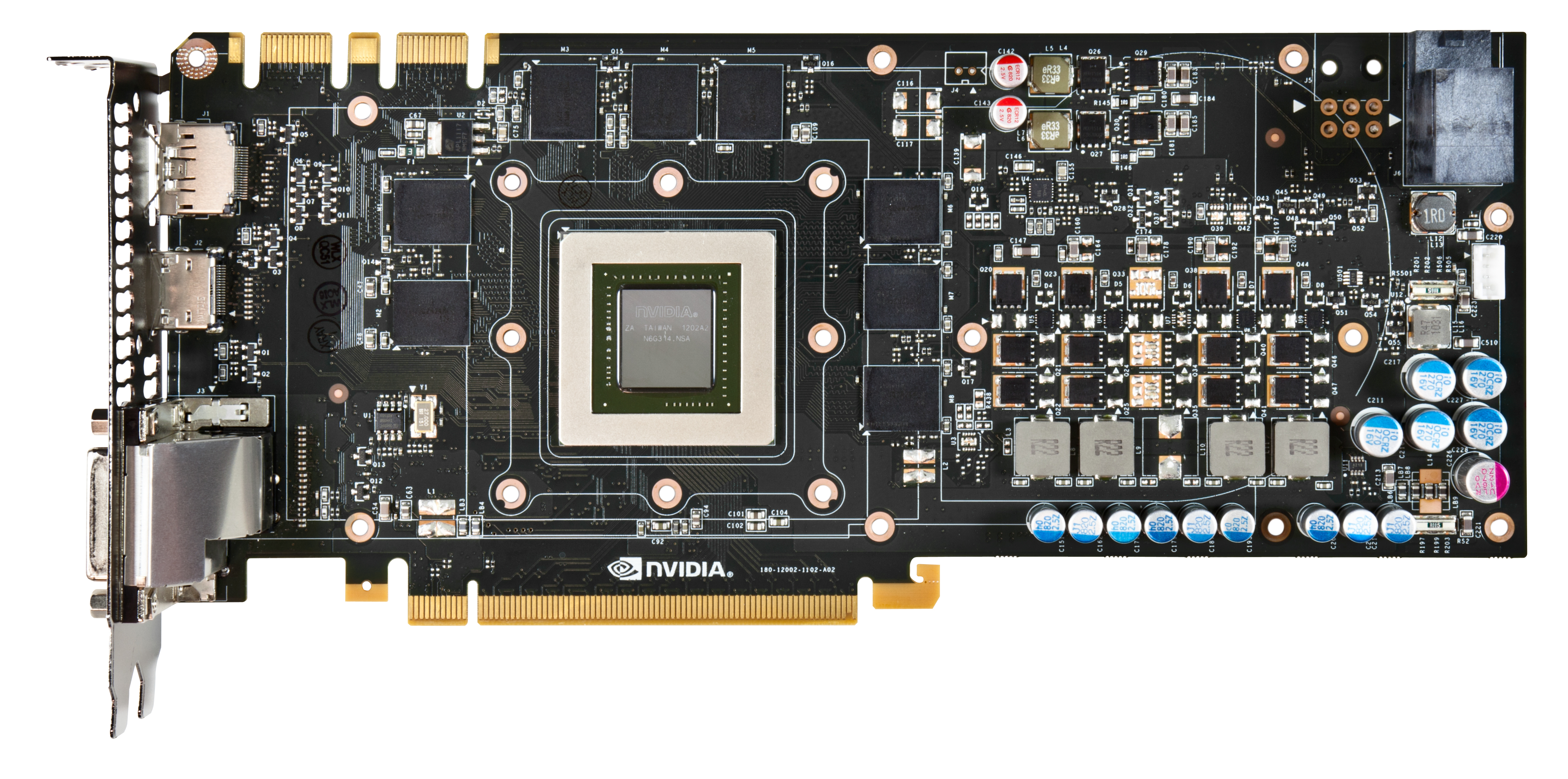
Moving on, when we remove the shroud on the GTX 680 we see the fan, baseplate, and heatsink in full detail. NVIDIA is using an aluminum fin stacked heatsink, very similar to what we saw on the GTX 580. Underneath the heatsink NVIDIA is using a set of three heatpipes to transfer heat between the GPU and the heatsink. This is as opposed to the vapor chamber on the GTX 580, and while this setup doesn’t allow empirical testing, given the high efficiency of vapor chambers it’s likely that this isn’t quite as efficient, though to what degree we couldn’t say.
Finally, after removing the fan, baseplate, and heatsink, we can see the PCB in full detail. Unlike GF110 and GF114, GK104 is not capped with an IHS, allowing for the heatsink to directly come in contact with the GPU die. Meanwhile arranged around the GPU we can see the 8 2Gb GDDR5 RAM modules that give the GTX 680 its 2GB of RAM. These are Hynix R0C modules, which means they’re rated for 6GHz, the stock memory speed for the GTX 680. Overall the card measures 10” long with no overhang from the shroud, making it 0.5” shorter than the GTX 580.
Looking at the top of the card, as always we see the SLI connectors. Following in the footsteps of the GTX 580, the GTX 680 features 2 SLI connectors, allowing for up to 3-way SLI.
Meanwhile at the front of the card we see the I/O bracket. As we alluded to previously, the GTX 680 uses a stacked DVI design here; NVIDIA has done everything they can to keep the DVI ports at the very bottom of the card to avoid impeding airflow, but the upper DVI port still occupies roughly 40% of what would otherwise be the vent. Altogether the GTX 680 features 2 DL-DVI ports, a full size HDMI port, and a full size DisplayPort.
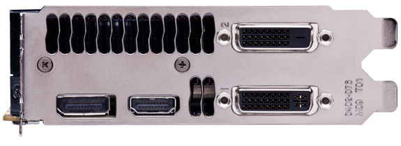
While NVIDIA has used DVI and HDMI ports for quite some time, this is the first time NVIDIA has included DIsplayPort on a reference design. Unfortunately we find that this ruffles our feathers a bit, although this isn’t strictly NVIDIA’s fault. As we’ve covered in the past, DisplayPort comes in both a full size and miniDP configuration – AMD in particular has used miniDP since the Radeon HD 6800 series in 2010. And while we’re happy to see DisplayPort finally make it into an NVIDIA reference design, the fact that it’s a full size DisplayPort is less than encouraging because at this point in time DisplayPort has largely been replaced by miniDP.
Ultimately the fault for this lies more with the VESA than NVIDIA, but it’s indicative of a larger problem in the DisplayPort community in that both full size DP and miniDP are equally valid and equally capable ports. While full size DisplayPort has the distinction of coming first, thanks in large part to Apple it has largely been displaced by miniDP as the most common variant on source devices. The problem with this is that both miniDP and DisplayPort are now in wide use; wide, redundant use.
At this point desktop computers and video cards coming with full size DisplayPorts is silly at best, and frustrating at worst. The laptop guys aren’t going to give up miniDP due to the space savings, and there’s no significantly good reason to use DisplayPort on desktops when miniDP offers the same functionality. We would rather see the PC industry standardize on miniDP across all source devices, and thereby eliminate any ambiguity with regards to what cables or adaptors are necessary. DisplayPort adoption has been slow enough – having 2 variants of the port on source devices only makes it more confusing for everyone.
Finally, while we’re on the subject of display connectivity we quickly took a look at how the idle clockspeeds of GTX 680 are impacted by the use of multiple displays. With 2 displays GTX 680 can utilize its full idle clocks, but only if both displays are connected via a TMDS type connection (DVI/HDMI) and run with identical timings. But if different timings are used or if one display is connected via DisplayPort, then the GTX 680 will shift to its low power 3D clocks. However if we expand that to 3 monitors and enable NVIDIA Surround, then the GTX 680 can operate at full idle regardless of whether DisplayPort is used or not.


404 Comments
View All Comments
CeriseCogburn - Tuesday, March 27, 2012 - link
What you're saying is true for amd cards, and is severe in CF, but true across the board.Lower clocked cpu system, better results from Nvidia.
bozolino - Monday, March 26, 2012 - link
I dont know whats happening. I have a gtx 560 2win and wanted to compare it to the 680 and see if its worth the replace but the charts cant be compared, for example:http://www.anandtech.com/show/5048/evgas-geforce-g...
This review uses an i7 3xxx while the older uses an i7 720, how can the older cpu performs better than the new one?? Something is very odd....
I wish they had used same computer as vga test bench, so we could compare all the results together....
Sharpie - Monday, March 26, 2012 - link
Its about design trade offs, you can increase the memory speed if you have a narrow bus to get the same throughput of something with lower clock speed and a large bus. all depeends on the architectural design so arguing about clock numbers is pointless generally speaking unless you are comparing apples to apples. Comapring an NVidia chip to an ATI chip is apples to oranges. Yes, im an engineer.CeriseCogburn - Tuesday, March 27, 2012 - link
Oh I get it you're in some pretend world where the card companies are not "fanboy compared" in the article itself.Once the amd card loses, and someone tells the truth about that, it's trolling or fanboy right ?
If an amd fan lies, it's "a good opinion".
If an amd fan liar gets corrected, that's "taking it too far" into "fanboy".
Once aghain, telling the truth on the two competing cards is forbidden only if it's an Nvidia advantage - then WE MUST OMIT the AMD card from the analysis, right ?
I think you might as well NEVER read another article on a card launch at this site, if you intend to stick to your RUDE comment.
CeriseCogburn - Tuesday, March 27, 2012 - link
Heck you didn't read this article nor many others then that say and prove the exact thing.I'm sure it will never make sense to you.
SlyNine - Friday, April 27, 2012 - link
Actually, I'm pretty sure it's you that doesn't understand the DX API. The CPU's are doing roughly the same thing for both videocards. Cept when it comes to processing the Drivers.CeriseCogburn - Tuesday, March 27, 2012 - link
The GTX690 currently holds the world record with a 1,900mhz overclock, and is gaining easily 15% with noob out of box overlclocks, and reaching very high memory clocks as well as 1,300+ core, I've seen 1,420 on air, and overclocked models are on their way....So much for that fud about 7970... it's FUD FUD and pure FUD.
blanarahul - Tuesday, March 27, 2012 - link
GTX 690????blanarahul - Tuesday, March 27, 2012 - link
Smart move by NVIDIA. Make a single gpu powerful graphics card to battle the Dual Tahiti monster. Judging by how they are doing the GTX 680 it should have the following specs:-4.72 billion transiostors
2048 CUDA Cores
384-bit memory bus width
3 GB VRAM
600-700 USD
TDP of 225-250W
If the clock speeds high enough, it will be quite a match for the 7990!
The reason i think it will be a single GPU card is because GTX 680=2x GTX 560 Ti.
So it should be GTX 690=2x GTX 580.
CeriseCogburn - Tuesday, March 27, 2012 - link
The release date of the 7970 was jan 11th, 2.5 months is opverstating in AMD's favor...Nothing like not knowing what you're talking about huh.
7970's have come down in price a bit, but you still will find them for much more than $569 at an awful lot of USA online places.