NVIDIA GeForce GTX 680 Review: Retaking The Performance Crown
by Ryan Smith on March 22, 2012 9:00 AM ESTThe Kepler Architecture: Fermi Distilled
As GPU complexity has increased over the years, so has the amount of time it takes to design a GPU. Specific definitions vary on what constitutes planning, but with modern GPUs such as Fermi, Kepler, and Tahiti planning basically starts 4+ years ahead of time. At this point in time GPUs have a similarly long development period as CPUs, and that alone comes with some ramifications.
The biggest ramification of this style of planning is that because designing a GPU is such a big undertaking, it’s not something you want to do frequently. In the CPU space Intel has their tick-tock strategy, which has Intel making incremental architecture updates every 2 years. While in the GPU space neither NVIDIA or AMD have something quite like that – new architectures and new process nodes still tend to premiere together – there is a similar need to spread out architectures over multiple years.
For NVIDIA, Kepler is the embodiment of that concept. Kepler brings with it some very important architectural changes compared to Fermi, but at the same time it’s still undeniably Fermi. From a high level overview Kepler is identical to Fermi: it’s still organized into CUDA cores, SMs, and GPCs, and how warps are executed has not significantly changed. Nor for that matter has the rendering side significantly changed, with rendering still being handled in a distributed fashion through raster engines, polymorph engines, and of course the ROPs. The fact that NVIDIA has chosen to draw up Kepler like Fermi is no accident or coincidence; at the end of the day Kepler is the next generation of Fermi, tweaked and distilled to improve on Fermi’s strengths while correcting its weaknesses.
For our look at Kepler’s architecture, we’re going to be primarily comparing it to GF114, aka Fermi Lite. As you may recall, with Fermi NVIDIA had two designs: a multipurpose architecture for gaming and graphics (GF100/GF110), and a streamlined architecture built with a stronger emphasis on graphics than compute (GF104, etc) that was best suited for use in consumer graphics. As hinted at by the name alone, GK104 is designed to fill the same consumer graphics role as GF114, and consequently NVIDIA built GK104 off of GF114 rather than GF110.
So what does GK104 bring to the table? Perhaps it’s best to start with the SMs, as that’s where most of the major changes have happened.
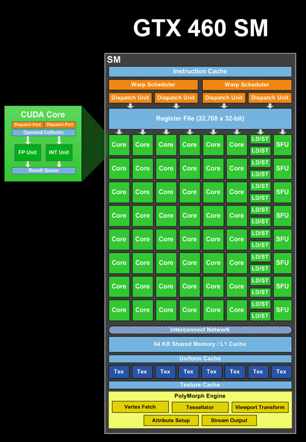
In GF114 each SM contained 48 CUDA cores, with the 48 cores organized into 3 groups of 16. Joining those 3 groups of CUDA cores were 16 load/store units, 16 interpolation SFUs, 8 special function SFUs, and 8 texture units. Feeding all of those blocks was a pair of warp schedulers, each of which could issue up to 2 instructions per core clock cycle, for a total of up to 4 instructions in flight at any given time.
GF104/GF114 SM Functional Units
- 16 CUDA cores (#1)
- 16 CUDA cores (#2)
- 16 CUDA cores, FP64 capable (#3)
- 16 Load/Store Units
- 16 Interpolation SFUs (not on NVIDIA's diagrams)
- 8 Special Function SFUs
- 8 Texture Units
Within the SM itself different units operated on different clocks, with the schedulers and texture units operating on the core clock, while the CUDA cores, load/store units, and SFUs operated on the shader clock, which ran at twice the core clock. As NVIDIA’s warp size is 32 threads, if you do the quick math you realize that warps are twice as large as any block of functional units, which is where the shader clock comes in. With Fermi, a warp would be split up and executed over 2 cycles of the shader clock; 16 threads would go first, and then the other 16 threads over the next clock. The shader clock is what allowed NVIDIA to execute a full warp over a single graphics clock cycle while only using enough hardware for half of a warp.
So how does GK104 change this? The single most important aspect of GK104, the thing that in turn dictates the design of everything else, is that NVIDIA has dropped the shader clock. Now the entire chip, from ROP to CUDA core, runs on the same core clock. As a consequence, rather than executing two half-warps in quick succession GK104 is built to execute a whole warp at once, and GK104’s hardware has changed dramatically as a result.
Because NVIDIA has essentially traded a fewer number of higher clocked units for a larger number of lower clocked units, NVIDIA had to go in and double the size of each functional unit inside their SM. Whereas a block of 16 CUDA cores would do when there was a shader clock, now a full 32 CUDA cores are necessary. The same is true for the load/store units and the special function units, all of which have been doubled in size in order to adjust for the lack of a shader clock. Consequently, this is why we can’t just immediately compare the CUDA core count of GK104 and GF114 and call GK104 4 times as powerful; half of that additional hardware is just to make up for the lack of a shader clock.
But of course NVIDIA didn’t stop there, as swapping out the shader clock for larger functional units only gives us the same throughput in the end. After doubling the size of the functional units in a SM, NVIDIA then doubled the number of functional units in each SM in order to grow the performance of the SM itself. 3 groups of CUDA cores became 6 groups of CUDA cores, 2 groups of load/store units, 16 texture units, etc. At the same time, with twice as many functional units NVIDIA also doubled the other execution resources, with 2 warp schedulers becoming 4 warp schedulers, and the register file being doubled from 32K entries to 64K entries.
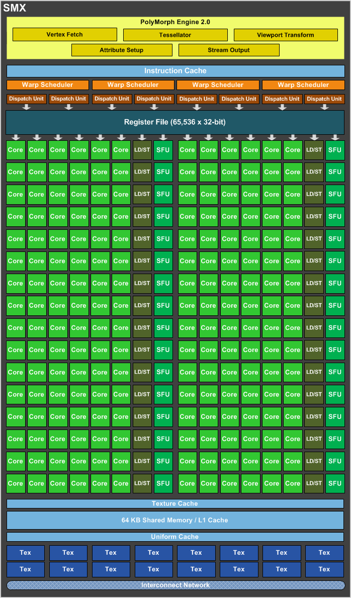
Ultimately where the doubling of the size of the functional units allowed NVIDIA to drop the shader clock, it’s the second doubling of resources that makes GK104 much more powerful than GF114. The SMX is in nearly every significant way twice as powerful as a GF114 SM. At the end of the day NVIDIA already had a strong architecture in Fermi, so with Kepler they’ve gone and done the most logical thing to improve their performance: they’ve simply doubled Fermi.
Altogether the SMX now has 15 functional units that the warp schedulers can call on. Each of the 4 schedulers in turn can issue up to 2 instructions per clock if there’s ILP to be extracted from their respective warps, allowing the schedulers as a whole to issue instructions to up to 8 of the 15 functional units in any clock cycle.
GK104 SMX Functional Units
- 32 CUDA cores (#1)
- 32 CUDA cores (#2)
- 32 CUDA cores (#3)
- 32 CUDA cores (#4)
- 32 CUDA cores (#5)
- 32 CUDA cores (#6)
- 16 Load/Store Units (#1)
- 16 Load/Store Units (#2)
- 16 Interpolation SFUs (#1)
- 16 Interpolation SFUs (#2)
- 16 Special Function SFUs (#1)
- 16 Special Function SFUs (#2)
- 8 Texture Units (#1)
- 8 Texture Units (#2)
- 8 CUDA FP64 cores
While that covers the operation of the SMX in a nutshell, there are a couple of other things relating to the SMX that need to be touched upon. Because NVIDIA still only has a single Polymorph Engine per SMX, the number of Polymorph Engines hasn’t been doubled like most of the other hardware in an SMX. Instead the capabilities of the Polymorph Engine itself have been doubled, making each Polymorph Engine 2.0 twice as powerful as a GF114 Polymorph Engine. In absolute terms, this means each Polymorph Engine can now spit out a polygon in 2 cycles, versus 4 cycles on GF114, for a total of 4 polygons/clock across GK104.
The other change coming from GF114 is the mysterious block #15, the CUDA FP64 block. In order to conserve die space while still offering FP64 capabilities on GF114, NVIDIA only made one of the three CUDA core blocks FP64 capable. In turn that block of CUDA cores could execute FP64 instructions at a rate of ¼ FP32 performance, which gave the SM a total FP64 throughput rate of 1/12th FP32. In GK104 none of the regular CUDA core blocks are FP64 capable; in its place we have what we’re calling the CUDA FP64 block.
The CUDA FP64 block contains 8 special CUDA cores that are not part of the general CUDA core count and are not in any of NVIDIA’s diagrams. These CUDA cores can only do and are only used for FP64 math. What's more, the CUDA FP64 block has a very special execution rate: 1/1 FP32. With only 8 CUDA cores in this block it takes NVIDIA 4 cycles to execute a whole warp, but each quarter of the warp is done at full speed as opposed to ½, ¼, or any other fractional speed that previous architectures have operated at. Altogether GK104’s FP64 performance is very low at only 1/24 FP32 (1/6 * ¼), but the mere existence of the CUDA FP64 block is quite interesting because it’s the very first time we’ve seen 1/1 FP32 execution speed. Big Kepler may not end up resembling GK104, but if it does then it may be an extremely potent FP64 processor if it’s built out of CUDA FP64 blocks.
Moving on, now that we’ve dissected GK104’s SMX, let’s take a look at the bigger picture. Above the SM(X)es we have the GPCs. The GPCs contain multiple SMs and more importantly the Raster Engine responsible for all rasterization. As with the many other things being doubled in GK104, the number of GPCs has been doubled from 2 to 4, thereby doubling the number of Raster Engines present. This in turn changes the GPC-to-SM(X) ratio from 1:4 on GF114 to 1:2 on GK104. The ratio itself is not particularly important, but it’s worth noting that it does take more work for NVIDIA to lay down and connect 4 GPCs than it does 2 GPCs.
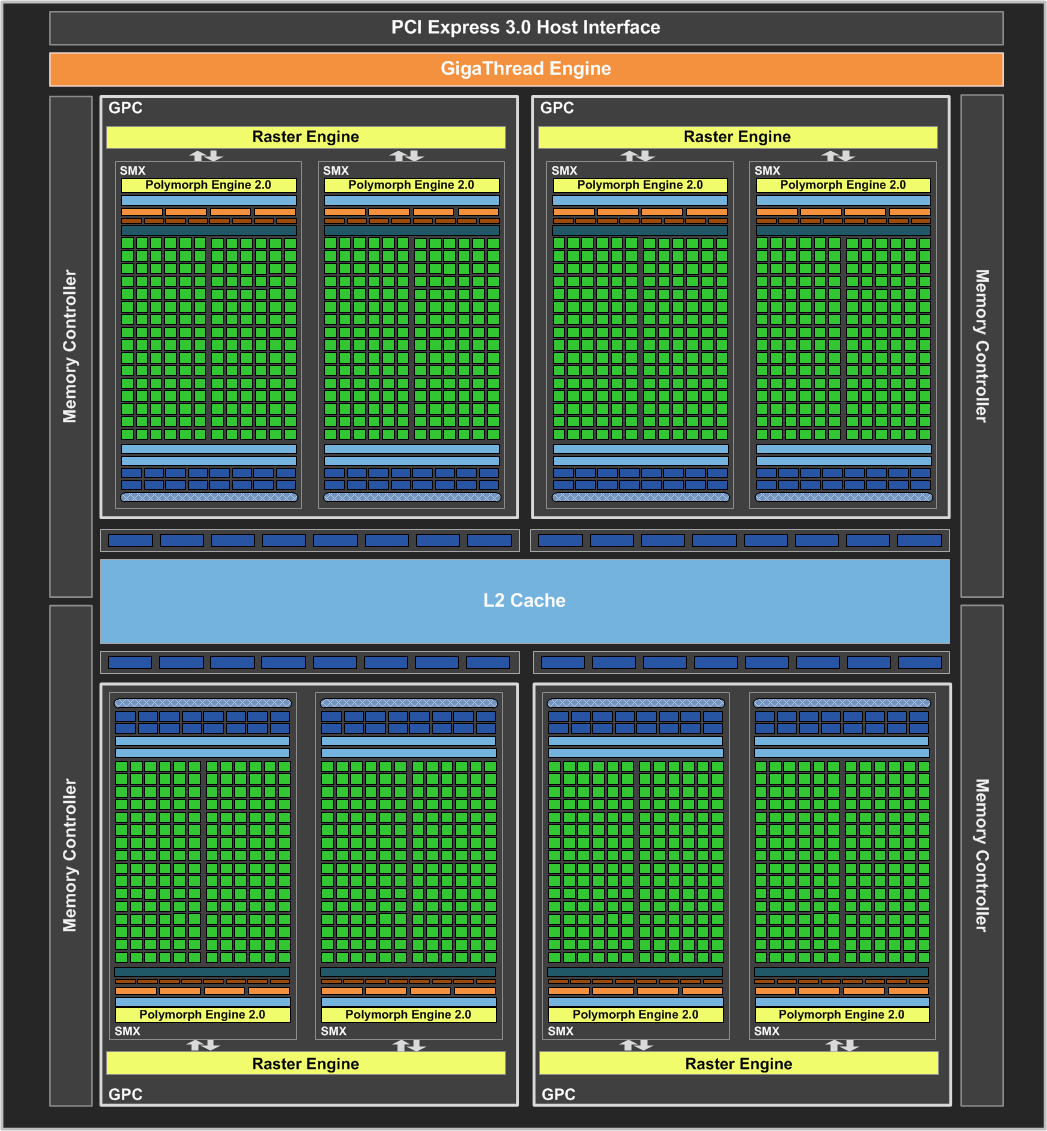
Last, but certainly not least is the complete picture. The 4 GPCs are combined with the rest of the hardware that makes GK104 tick, including the ROPs, the memory interfaces, and the PCIe interface. The ROPs themselves are virtually identical to those found on GF114; theoretical performance is the same, and at a lower level the only notable changes are an incremental increase in compression efficiency, and improved polygon merging. Similarly, the organization of the ROPs has not changed either, as the ROPs are still broken up into 4 blocks of 8, with each ROP block tied to a 64 bit memory controller and 128KB of L2 cache. Altogether there are 32 ROPs, giving us 512KB of L2 cache and a 256bit memory bus.
On a final tangent, the memory controllers ended up being an unexpected achievement for NVIDIA. As you may recall, Fermi’s memory controllers simply never reached their intended targets – NVIDIA hasn’t told us what those targets were, but ultimately Fermi was meant to reach memory clocks higher than 4GHz. With GK104 NVIDIA has improved their memory controllers and then some. GK104’s memory controllers can clock some 50% higher than GF114’s, leading to GTX 680 shipping at 6GHz.
On a technical level, getting to 6GHz is hard, really hard. GDDR5 RAM can reach 7GHz and beyond on the right voltage, but memory controllers and the memory bus are another story. As we have mentioned a couple of times before, the memory bus tends to give out long before anything else does, which is what’s keeping actual shipping memory speeds well below 7GHz. With GK104 NVIDIA’s engineers managed to put together a chip and board that are good enough to run at 6GHz, and this alone is quite remarkable given how long GDDR5 has dogged NVIDIA and AMD.
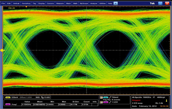
GK104 GDDR5 Signal Analysis
Perhaps the icing on the cake for NVIDIA though is how many revisions it took them to get to 6GHz: one. NVIDIA was able to get 6GHz on the very first revision of GK104, which after Fermi’s lackluster performance is a remarkable turn of events. And ultimately while NVIDIA says that they’re most proud of the end result of GK104, the fact of the matter is that everyone seems just a bit prouder of their memory controller, and for good reason.


404 Comments
View All Comments
Targon - Thursday, March 22, 2012 - link
Many people have been blasting AMD for price vs performance in the GPU arena in the current round of fighting. The thing is, until now, AMD had no competition, so it was expected that the price would remain high until NVIDIA released their new generation. So, expect lower prices from AMD to be released in the next week.You also fail to realize that with a 3 month lead, AMD is that much closer to the refresh parts being released that will beat NVIDIA for price vs. performance. Power draw may still be higher from the refresh parts, but that will be addressed for the next generation.
Now, you and others have been claiming that NVIDIA is somehow blowing AMD out of the water in terms of performance, and that is NOT the case. Yes, the 680 is faster, but isn't so much faster that AMD couldn't EASILY counter with a refresh part that catches up or beats the 680 NEXT WEEK. The 7000 series has a LOT of overclocking room there.
So, keep things in perspective. A 3 percent performance difference isn't enough to say that one is so much better than the other. It also remains to be seen how quickly the new NVIDIA parts will be made available.
SlyNine - Thursday, March 22, 2012 - link
I still blast them, I'm not happy with the price/performance increase of this generation at all.Unspoken Thought - Thursday, March 22, 2012 - link
Finally! Logic! But it still falls on deaf ears. We finally see both sides getting their act together to get minimum features sets in, and we can't see passed our own bias squabbles.How about we continue to push these manufactures in what we want and need most; more features, better algorithms, and last and most important, revolutionize and find new way to render, aside from vector based rendering.
Lets start incorporating high level mathematics for fluid dynamics and the such. They have already absorbed PhysX and moved to Direct Compute. Lets see more realism in games!
Where is the Technological Singularity when you need one.
CeriseCogburn - Thursday, March 22, 2012 - link
Well, the perspective I have is amd had a really lousy (without drivers) and short 2.5 months when the GTX580 wasn't single core king w GTX590 dual core king and the latter still is and the former has been replaced by the GTX680.So right now Nvidia is the asbolute king, and before now save that very small time period Nvidia was core king for what with the 580 .. 1.5 years ?
That perspective is plain fact.
FACTS- just stating those facts makes things very clear.
We already have heard the Nvidia monster die is afoot - that came out with "all the other lies" that turned out to be true...
I don't fail to realize anything - I just have a clear mind about what has happened.
I certainly hope AMD has a new better core slapped down very soon, a month would be great.
Until AMD is really winning, it's LOSING man, it's LOSING!
CeriseCogburn - Thursday, March 22, 2012 - link
Since amd had no competition for 2.5 months and that excuses it's $569.99 price, then certainly the $500 price on the GTX580 that had no competition for a full year and a half was not an Nvidia fault, right ? Because you're a fair person and "finally logic!" is what another poster supported you with...So thanks for saying the GTX580 was never priced too high because it has no competition for 1.5 years.
Unspoken Thought - Saturday, March 24, 2012 - link
Honestly the only thing I was supporting was the fact he is showing that perspective changes everything. a fact exacerbated when bickering over marginal differences that are driven by the economy when dealing with price vs performance.Both of you have valid arguments, but it sounds like you just want to feel better about supporting nVidia.
You should be able to see how AMD achieved its goals with nVidia following along playing leap frog. Looking at benchmarks, no it doesn't beat it in everything and both are very closely matched in power consumption, heat, and noise. Features are where nVidia shine and get my praise. but I would not fault you if you had either card.
CeriseCogburn - Friday, April 6, 2012 - link
Ok Targon, now we know TiN put the 1.3V core on the 680 and it OC'ed on air to 1,420 core, surpassing every 7970 1.3V core overclock out there.Furthermore, Zotac has put out the 2,000Ghz 680 edition...
So it appears the truth comes down to the GTX680 has more left in the core than the 7970.
Nice try but no cigar !
Nice spin but amd does not win !
Nice prediction, but it was wrong.
SlyNine - Thursday, March 22, 2012 - link
Go back and look at the benchmarks idiot. 7970 wins in some situations.SlyNine - Thursday, March 22, 2012 - link
In Crysis max, 7970 gets 36 FPS while the 680 only gets 30 FPS.Yes, some how the 7970 is losing. LOOK AT THE NUMBERS, HELLO!!???
Metro 2033 the 7970 gets 38 and the 680 gets 37. But yet in your eyes another loss for the 7970...
7970 kills it in certian GPU Compute, and has hardware H.264 encoding.
In a couple of games, which you already get massive FPS with both, the 680 boasts much much higher FPS. But than in games where you need the FPS the 7970 wins. Hmmm
But no no, you're right, the 680 is total elite top shit.
eddieroolz - Friday, March 23, 2012 - link
You pretty much admitted that 7970 loses in a lot of other cases by stating that:"7970 kills it in certain GPU compute..."
Adding the word modifier "certain" to describe a win is like admitting defeat in every other compute situation.
Even for the games, you can only mention 2 out of what, 6 games where 7970 wins by a <10% margin. Meanwhile, GTX 680 proceeds to maul the 7970 by >15% in at least 2 of the games.
Yes, 7970 is full of win, indeed! /s