The Apple iPad Review (2012)
by Vivek Gowri & Anand Lal Shimpi on March 28, 2012 3:14 PM ESTThe GPU
3D rendering is a massively parallel problem. Your GPU ultimately has to determine the color value of each pixel which may not remain constant between frames, at a rate of dozens of times per second. The iPad 2 had 786,432 pixels in its display, and by all available measures its GPU was more than sufficient to drive that resolution. The new iPad has 3.14 million pixels to drive. The iPad 2's GPU would not be sufficient.
When we first heard Apple using the term A5X to refer to the new iPad's SoC, I assumed we were looking at a die shrunk, higher clock version of the A5. As soon as it became evident that Apple remained on Samsung's 45nm LP process, higher clocks were out of the question. The only room for improving performance was to go wider. Thankfully, as 3D rendering is a massively parallel problem, simply adding more GPU execution resources tends to be a great way of dealing with a more complex workload. The iPad 2 shocked the world with its dual-core PowerVR SGX 543MP2 GPU, and the 3rd generation iPad doubled the amount of execution hardware with its quad-core PowerVR SGX 543MP4.
| Mobile SoC GPU Comparison | |||||||||||
| Adreno 225 | PowerVR SGX 540 | PowerVR SGX 543MP2 | PowerVR SGX 543MP4 | Mali-400 MP4 | Tegra 2 | Tegra 3 | |||||
| SIMD Name | - | USSE | USSE2 | USSE2 | Core | Core | Core | ||||
| # of SIMDs | 8 | 4 | 8 | 16 | 4 + 1 | 8 | 12 | ||||
| MADs per SIMD | 4 | 2 | 4 | 4 | 4 / 2 | 1 | 1 | ||||
| Total MADs | 32 | 8 | 32 | 64 | 18 | 8 | 12 | ||||
| GFLOPS @ 200MHz | 12.8 GFLOPS | 3.2 GFLOPS | 12.8 GFLOPS | 25.6 GFLOPS | 7.2 GFLOPS | 3.2 GFLOPS | 4.8 GFLOPS | ||||
| GFLOPS @ 300MHz | 19.2 GFLOPS | 4.8 GFLOPS | 19.2 GFLOPS |
38.4 GFLOPS |
10.8 GFLOPS | 4.8 GFLOPS | 7.2 GFLOPS | ||||
| GFLOPS As Shipped by Apple/ASUS | - | - | 16 GFLOPS | 32 GFLOPS | - | - |
12 GFLOPS |
||||
We see this approach all of the time in desktop and notebook GPUs. To allow games to run at higher resolutions, companies like AMD and NVIDIA simply build bigger GPUs. These bigger GPUs have more execution resources and typically more memory bandwidth, which allows them to handle rendering to higher resolution displays.
Apple acted no differently than a GPU company would in this case. When faced with the challenge of rendering to a 3.14MP display, Apple increased compute horsepower and memory bandwidth. What's surprising about Apple's move is that the A5X isn't a $600 desktop GPU, it's a sub 4W mobile SoC. And did I mention that Apple isn't a GPU company?
That's quite possibly the most impressive part of all of this. Apple isn't a GPU company. It's a customer of GPU companies like AMD and NVIDIA, yet Apple has done what even NVIDIA would not do: commit to building an SoC with an insanely powerful GPU.
I whipped up an image to help illustrate. Below is a representation, to-scale, of Apple and NVIDIA SoCs, their die size, and time of first product introduction:
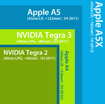
If we look back to NVIDIA's Tegra 2, it wasn't a bad SoC—it was basically identical in size to Apple's A4. The problem was that the Tegra 2 made its debut a full year after Apple's A4 did. The more appropriate comparison would be between the Tegra 2 and the A5, both of which were in products in the first half of 2011. Apple's A5 was nearly 2.5x the size of NVIDIA's Tegra 2. A good hunk of that added die area came from the A5's GPU. Tegra 3 took a step in the right direction but once again, at 80mm^2 the A5 was still over 50% larger.
The A5X obviously dwarfs everything, at around twice the size of NVIDIA's Tegra 3 and 33.6% larger than Apple's A5. With silicon, size isn't everything, but when we're talking about similar architectures on similar manufacturing processes, size does matter. Apple has been consistently outspending NVIDIA when it comes to silicon area, resulting in a raw horsepower advantage, which in turns results in better peak GPU performance.
Apple Builds a Quad-Channel (128-bit) Memory Controller
There's another side effect that you get by having a huge die: room for wide memory interfaces. Silicon layout is a balancing act. You want density to lower costs, but you don't want hotspots so you need heavy compute logic to be spread out. You want wide IO interfaces but you don't want them to be too wide because then you'll cause your die area to balloon as a result. There's only so much room on the perimeter of your SoC to get data out of the chip, hence the close relationship between die size and interface width.
Most mobile SoCs are equipped with either a single or dual-channel LP-DDR2 memory controller. Unlike in the desktop/notebook space where a single DDR2/DDR3 channel refers to a 64-bit wide interface, in the mobile SoC world a single channel is 32-bits wide. Both Qualcomm and NVIDIA use single-channel interfaces, with Snapdragon S4 finally making the jump to dual-channel this year. Apple, Samsung, and TI have used dual-channel LP-DDR2 interfaces instead.
With the A5X Apple did the unthinkable and outfitted the chip with four 32-bit wide LP-DDR2 memory controllers. The confirmation comes from two separate sources. First we have the annotated A5X floorplan courtesy of UBMTechInsights:
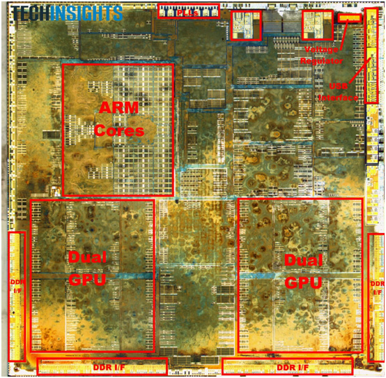
You can see the four DDR interfaces around the lower edge of the SoC. Secondly, we have the part numbers of the discrete DRAM devices on the opposite side of the motherboard. Chipworks and iFixit played the DRAM lottery and won samples with both Samsung and Elpida LP-DDR2 devices on-board, respectively. While both Samsung and Elpida do a bad job of updating public part number decoders, both strings match up very closely to 216-ball PoP 2x32-bit PoP DRAM devices. The part numbers don't match up exactly, but they are close enough that I believe we're simply looking at a discrete flavor of those PoP DRAM devices.
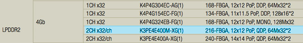
K3PE4E400M-XG is the Samsung part number for a 2x32-bit LPDDR2 device, K3PE4E400E-XG is the part used in the iPad. I've made bold the only difference.
A cross reference with JEDEC's LP-DDR2 spec tells us that there is an official spec for a single package, 216-ball dual-channel (2x32-bit) LP-DDR2 device, likely what's used here on the new iPad.
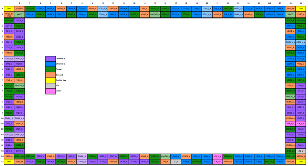
The ball out for a 216-ball, single-package, dual-channel (64-bit) LPDDR2 DRAM
This gives the A5X a 128-bit wide memory interface, double what the closest competition can muster and putting it on par with what we've come to expect from modern x86 CPUs and mainstream GPUs.
The Geekbench memory tests show no improvement in bandwidth, which simply tells us that the interface from the CPU cores to the memory controller hasn't seen a similar increase in width.
| Memory Bandwidth Comparison—Geekbench 2 | ||||||
| Apple iPad (3rd gen) | ASUS TF Prime | Apple iPad 2 | Motorola Xyboard 10.1 | |||
| Overall Memory Score | 821 | 1079 | 829 | 1122 | ||
| Read Sequential | 312.0 MB/s | 249.0 MB/s | 347.1 MB/s | 364.1 MB/s | ||
| Write Sequential | 988.6 MB/s | 1.33 GB/s | 989.6 MB/s | 1.32 GB/s | ||
| Stdlib Allocate | 1.95 Mallocs/sec | 2.25 Mallocs/sec | 1.95 Mallocs/sec | 2.2 Mallocs/sec | ||
| Stdlib Write | 2.90 GB/s | 1.82 GB/s | 2.90 GB/s | 1.97 GB/s | ||
| Stdlib Copy | 554.6 MB/s | 1.82 GB/s | 564.5 MB/s | 1.91 GB/s | ||
| Overall Stream Score | 331 | 288 | 335 | 318 | ||
| Stream Copy | 456.4 MB/s | 386.1 MB/s | 466.6 MB/s | 504 MB/s | ||
| Stream Scale | 380.2 MB/s | 351.9 MB/s | 371.1 MB/s | 478.5 MB/s | ||
| Stream Add | 608.8 MB/s | 446.8 MB/s | 654.0 MB/s | 420.1 MB/s | ||
| Stream Triad | 457.7 MB/s | 463.7 MB/s | 437.1 MB/s | 402.8 MB/s | ||
Although Apple designed its own memory controller in the A5X, you can see that all of these A9 based SoCs deliver roughly similar memory performance. The numbers we're showing here aren't very good at all. Even though Geekbench has never been good at demonstrating peak memory controller efficiency to begin with, the Stream numbers are very bad. ARM's L2 cache controller is very limiting in the A9, something that should be addressed by the time the A15 rolls around.
Firing up the memory interface is a very costly action from a power standpoint, so it makes sense that Apple would only want to do so when absolutely necessary. Furthermore, notice how the memory interface moved from being closer to the CPU in A4/A5 to being adjacent to the GPU in the A5X. It would appear that only the GPU has access to all four channels.


234 Comments
View All Comments
JasperJanssen - Sunday, April 15, 2012 - link
The iPad uses the same battery technology as the iPhone and the MacBook Air — flat LiPo cells. As owner of all three (iPad 1, 3, iPhone 3G, 3GS, 4, 4S, MacBook Air 13" mid-2011) I can tell you that yes, this is fine. The absolute least degradation of your battery capacity would be to leave it around 70% full and never use the device.Second best is to not let it drain down too far, say not under 20-30%. Third best from a capacity standpoint but by far the best in user experience is to not worry about it. All of my devices (iPhone in front, of course) drain to under thirty percent on a regular basis. The one I've had and used longest, the iPad (1st gen), hasn't had a perceptible decrease in battery life after two years, although I admit I haven't run actual tests.
If you do manage to use it so much the battery gets tired, a replacement out of warranty from Apple costs only $99+shipping, slightly more than DIY but a lot less hassle. Currently that service is available for all iPhones including the 2G, so not very likely to be unavailable during the useful life of an iPad.
evolucion8 - Thursday, August 1, 2013 - link
I love your articles and site, I wish I could say the same thing to your forums, most admins there are just doing their own whatever it feels like, threating and offending people with private messages and turning your forums into a monkey sling cr*p fest.sunilt - Friday, July 4, 2014 - link
Hi Anand,Which application you used for downloading with constant speed?
marjoriejackson66 - Thursday, March 22, 2018 - link
Apple product is really helpful and reliable to the user. I always recommended these products.