The Xeon E5-2600: Dual Sandy Bridge for Servers
by Johan De Gelas on March 6, 2012 9:27 AM EST- Posted in
- IT Computing
- Virtualization
- Xeon
- Opteron
- Cloud Computing
Measuring Real-World Power Consumption
The Equal Workload (EWL) version of vApus FOS is very similar to our previous vApus Mark II "Real-world Power" test. To create a real-world “equal workload” scenario, we throttle the number of users in each VM to a point where you typically get somewhere between 20% and 80% CPU load on a modern dual CPU server. The amount of requests is the same for each system, hence "equal workload". The CPU load is typically around 30-50%, with peaks up to 65% (for more info see here). At the end of the test, we get to a low 10%, which is ideal for the machine to boost to higher CPU clocks (Turbo) and race to idle.
We used the "Balanced" power policy and enabled C-states as the current ESXi settings make poor use of the C6 capabilities of the latest Opterons and Xeons.
First let's check out the response times.
| vApus FOS Response times (ms) | ||||||||
| CPU | PhpBB1 | PHPBB2 | MySQL OLAP | Zimbra | ||||
| AMD Opteron 6276 | 101 | 30 | 3.8 | 41 | ||||
| AMD Opteron 6174 | 118 | 41 | 3.8 | 45 | ||||
| Intel Xeon X5650 | 45 | 18 | 2.4 | 29 | ||||
| Intel Xeon E5-2660 | 41 | 18 | 2.5 | 25 | ||||
| Intel Xeon E5-2690 | 27 | 14 | 2.3 | 23 | ||||
It's worth noting that enabling the C-states in ESXi improves the performance/watt ratio of the Opteron 6276 quite a bit. Not only is the power consumption lower (see below), but enabling C6 allows higher turbo clocks, which in turn benefits response times. Compared to our previous test (standard out of the box "Balanced") all response times improve by 10% except for MySQL (which is already very low).
Even with that improvement however it is not enough to beat the Xeon E5. The Xeon E5 delivers extremely low response times....
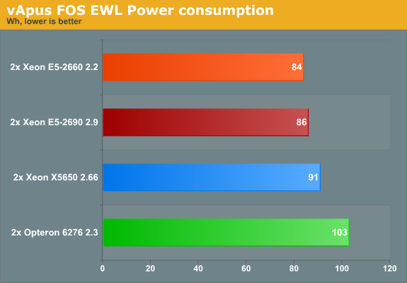
... while sipping very little power, despite being run inside a feature rich server. Kudos to Intel for a job very well done.


81 Comments
View All Comments
BSMonitor - Tuesday, March 6, 2012 - link
My question as well.What is the Intel roadmap for Ivy Bridge in this arena. Would be the same timeframe as IVB-E I would guess.
Wondering if my Intel dividends will pile up enough for me to afford one! Haha
devdeepc - Friday, September 2, 2016 - link
Based on the paper specs, AMD's 6276, 6274 and Intel's 2640 and 2630 are in a neck-and-neck race.fredisdead - Saturday, April 7, 2012 - link
From the 'article' .....'The Opteron might also have a role in the low end, price sensitive HPC market, where it still performs very well. It won't have much of chance in the high end clustered one as Intel has the faster and more power efficient PCIe interface'
Well, if that's the case, why exactly would AMD be scoring so many design wins with Interlagos. Including this one ...
http://www.pcmag.com/article2/0,2817,2394515,00.as...
http://www.eweek.com/c/a/IT-Infrastructure/Cray-Ti...
U think those guys at Cray were going for low performance ? In fact, seems like AMD has being rather cleaning up in the HPC market since the arrival of Interlagos. And the markets have picked up on it, AMD stock is thru the roof since the start of the year. Or just see how many Intel processors occupy the the top 10 supercomputers on the planet. Nuff said ...
iwod - Tuesday, March 6, 2012 - link
And not find a single comment on how and why "making this CPU quite a challenge, even for Intel."In my view It seems Intel is now using Server Market and Atom / SoC for their 32nm capacity when ever they introduce a new node in consumer products.
extide - Tuesday, March 6, 2012 - link
A large part of Intel's long-term strategies include keeping the fabs occupied.Latest gen fabs (currently 22nm) produce bleeding edge cpu's, usually in the consumer space
One gen back (32nm) produces server/workstation/mobile cpus
two gens back (45nm) produces other things like chipsets, and possibly itanium chips
even three gens back (65nm) probably still exists in some places making some chipsets as well.
Their goal is to as much use as possible from their investment into building the fabs themselves.
Kevin G - Tuesday, March 6, 2012 - link
65 nm is still used for Itanium, though the Poulson chip is due sometime this year made on a 32 nm process. If you want to compare die sizes, the 65 nm Tukwila design is 699 mm^2 in size.The main reason why 32 nm Sandybridge-E has been released so close to the release of 22 nm Ivy Bridge chips is that the initial Ivy Bridge chips are consumer centric. Intel performs additional testing on its server centric designs. This is particularly true as Sandybridge-E is not just replacing the dual socket Westmere-EP chips but some of the quad socket Westmere-EX market. RAS demands jump from going from dual to quad socket and that is reflected in additional testing. Implementing PCI-E 3.0 and QPI 1.1 also contributed to the time for additional testing.
Though you are correct that Intel does uses its older process nodes for various chipsets and IO chips. However, as Intel is marching toward SoC designs, the actual utility of keeping these older process nodes in action is decreasing.
meloz - Tuesday, March 6, 2012 - link
>And not find a single comment on how and why "making this CPU quite a challenge, even for Intel."Because it is such a massive die? 416 mm²? Large dies usually have a lower yield, and Intel's 32 nm process is still cutting edge (if only for a few more weeks, heh).
Look at how TSMC, Global Flounderings et al are struggling. An impressive achievement by Intel.
MrSpadge - Tuesday, March 6, 2012 - link
A significant amount of functionality has been added to the SB cores, and Intel can't afford mistakes in such CPUs.BSMonitor - Tuesday, March 6, 2012 - link
More than that though, the SNB-E, Xeon E cores are not duplicates of the SNB desktop cores.Look at Anand's die shot of SNB-E, vs die shot of SNB. The CPU cores, L3 cache, controllers, are arranged completely different. Which makes sense as SNB-E doesn't have to deal with 40% of the die being GPU transistors. So, what we have now with Intel is two completely different dies between Xeon/SNB-E and Core. The individual CPU cores are the same, but the rest of the die is completely different.
SNB-E:
http://www.anandtech.com/show/5091/intel-core-i7-3...
SNB:
http://www.anandtech.com/show/4083/the-sandy-bridg...
cynic783 - Tuesday, March 6, 2012 - link
omg these benches are so biased it's not even funny. everyone knows amd offers clock-for-clock more punch than intel and lower power as well