Intel's Medfield & Atom Z2460 Arrive for Smartphones: It's Finally Here
by Anand Lal Shimpi on January 10, 2012 8:00 PM ESTThe CPU
Medfield is the platform, Penwell is the SoC and the CPU inside Penwell is codenamed Saltwell. It's honestly not much different than the Bonnell core used in the original Atom, although it does have some tweaks for both power and performance.
Almost five years ago I wrote a piece on the architecture of Intel's Atom. Luckily (for me, not Intel), Atom's architecture hasn't really changed over the years so you can still look back at that article and have a good idea of what is at the core of Medfield/Penwell. Atom is still a dual-issue, in-order architecture with Hyper Threading support. The integer pipeline is sixteen stages long, significantly deeper than the Cortex A9's. The longer pipeline was introduced to help reduce Atom's power consumption by lengthening some of the decode stages and increasing cache latency to avoid burning through the core's power budget. Atom's architects, similar to those who worked on Nehalem, had the same 2:1 mandate: every new feature added to the processor's design had to deliver at least a 2% increase in performance for every 1% increase in power consumption.
Atom is a very narrow core as the diagram below will show:
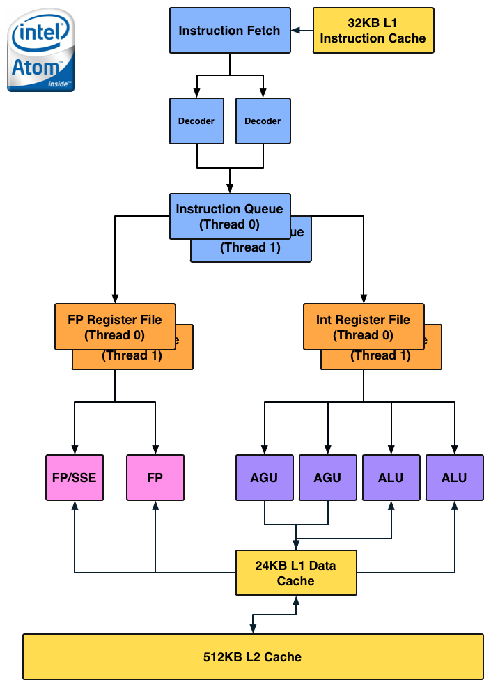
There are no dedicated integer multiply or divide units, that's all shared with the FP hardware. Intel duplicated some resources (e.g. register files, queues) to enable Hyper Threading support, but stopped short of increasing execution hardware to drive up efficiency. The tradeoff seems to have worked because Intel is able to deliver performance better than a dual-core Cortex A9 from a single HT enabled core. Intel also lucks out because while Android is very well threaded, not all tasks will continually peg both cores in a dual-core A9 machine. At higher clock speeds (1.5GHz+) and with heavy multi-threaded workloads, it's possible that a dual-core Cortex A9 could outperform (or at least equal) Medfield but I don't believe that's a realistic scenario.
Architecturally the Cortex A9 doesn't look very different from Atom:
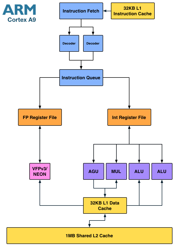
Here we see a dedicated integer multiply unit (shared with one of the ALU ports) but only a single port for FP/NEON. It's clear that the difference between Atom and the Cortex A9 isn't as obvious at the high level. Instead it's the lower level architectural decisions that gives Intel a performance advantage.
Where Intel is in trouble is if you look at the Cortex A15:
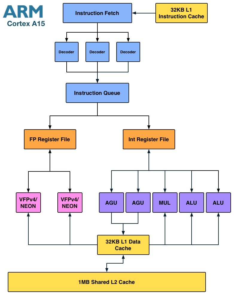
The A15 is a far more modern design, also out of order but much wider than A9. I fully expect that something A15-class can outperform Medfield, especially if the former is in a dual-core configuration. Krait falls under the A15-class umbrella so I believe Medfield has the potential to lose its CPU performance advantage within a couple of quarters.
Enhancements in Saltwell
Although the CPU core is mated to a 512KB L2 cache, there's a separate 256KB low power SRAM that runs on its own voltage plane. This ULP SRAM holds CPU state and data from the L2 cache when the CPU is power gated in the deepest sleep state. The reasoning for the separate voltage plane is simple. Intel's architects found that the minimum voltage for the core was limited by Vmin for the ULP SRAM. By putting the two on separate voltage planes it allowed Intel to bring the CPU core down to a lower minimum power state as Vmin for the L2 is higher than it is for the CPU core itself. The downside to multiple power islands is an increase in die area. Since Medfield is built on Intel's 32nm LP process while the company transitions to 22nm, spending a little more on die area to build more power efficient SoCs isn't such a big deal. Furthermore, Intel is used to building much larger chips, making Medfield's size a relative nonissue for the company.
The die size is actually very telling as it's a larger SoC than a Tegra 2 with two Cortex A9s despite only featuring a single core. Granted the rest of the blocks around the core are different, but it goes to show you that the CPU core itself (or number of cores) isn't the only determination of the die size of an SoC.
The performance tweaks come from the usual learnings that take place over the course of any architecture's lifespan. Some instruction scheduling restrictions have been lifted, memory copy performance is up, branch predictor size increased and some microcode flows run faster on Saltwell now.
Clock Speeds & Turbo
Medfield's CPU core supports several different operating frequencies and power modes. At the lowest level is its C6 state. Here the core and L2 cache are both power gated with their state is saved off in a lower power on-die SRAM. Total power consumption in C6 of the processor island is effectively zero. This isn't anything new, Intel has implemented similar technologies in desktops since 2008 (Nehalem) and notebooks since 2010 (Arrandale).
When the CPU is actually awake and doing something however it has a range of available frequencies: 100MHz all the way up to 1.6GHz in 100MHz increments.
The 1.6GHz state is a burst state and shouldn't be sustained for long periods of time, similar to how Turbo Boost works on Sandy Bridge desktop/notebook CPUs. The default maximum clock speed is 1.3GHz, although just as is the case with Turbo enabled desktop chips, you can expect to see frequencies greater than 1.3GHz on a fairly regular basis.
Power consumption along the curve is all very reasonable:
| Medfield CPU Frequency vs. Power | ||||||
| 100MHz | 600MHz | 1.3GHz | 1.6GHz | |||
| SoC Power Consumption | ~50mW | ~175mW | ~500mW | ~750mW | ||
Since most ARM based SoCs draw somewhere below 1W under full load, these numbers seem to put Medfield in line with its ARM competitors - at least on the CPU side.
It's important to pay attention to the fact that we're dealing with similar clock frequencies to what other Cortex A9 vendors are currently shipping. Any performance advantages will either be due to Medfield boosting up to 1.6GHz for short periods of time, inherently higher IPC and/or a superior cache/memory interface.


164 Comments
View All Comments
stadisticado - Wednesday, January 11, 2012 - link
I think dealcorn is being a bit hyperbolic. That said, even 'competitive' from Intel has to be a big warning sign for sellers of ARM chips.dealcorn - Wednesday, January 11, 2012 - link
I may be wrong and this will be measured by independent observers in due course, but I had no intent of being hyperbolic.If you look at the investor' chart on the first page of the article (where Anand says he knows who they are and what the power ratings are) Medfield ranks first in performance on all 3 tests. On economy it scores 2/6 twice and 3/6 once. When I look at how much they won by and how much they did not win by, my visual computer says "superior". Look at the pictures yourself and exercise your own judgment.
aury - Wednesday, January 11, 2012 - link
"intel did it"Uhm, you might like to show some side by side comparisons of that phone next to an actual phone instead of just the front.
The phone is about twice as thick as a normal phone, it has actual heat disappating sections, which means the chip is likely much hotter than an A9.
All the tests you show are the same ones intel shows on their CES pamflet, i.e. they are freaking useless, since they wouldn't put tests up there that didn't show them at an advantage.
This is not "intel did it", not by a long shot.
Anand Lal Shimpi - Wednesday, January 11, 2012 - link
iPhone 4S thickness: 9.3mm, Medfield reference design thickness: 9.5mm.There's apparently a thinner version but I don't believe the form factor is the issue anymore.
Take care,
Anand
jjj - Wednesday, January 11, 2012 - link
I wouldn't trust Intel data but we'll see,waiting eagerly for real products and real tests,just wish you were more objective when it comes to Intel.The ref platform is rather fat and the battery smaller than what most high end smartphones have so i wouldn't call it sweet.
The partnerships are ,hmm,rather interesting.Lenovo is not exactly a phone maker and while they might shift some volume in China they are not the ideal partner (and they can be payed off with some price cuts and marketing $). Moto AKA Google might have other reasons to do this. Samsung is starting to be too big and Intel competing in this space might slow them down somewhat and Google has no interest in not beeing present on x86 when they scale Android up so another favour after the Google TV deal would not be out of the question.Also with the Moto deal,Intel hurt Nvidia since they are the ones that got kicked out to make room for Intel.
At least ,if the numbers are even somewhat close to reality they could have a good product on 22nm.
aury - Wednesday, January 11, 2012 - link
What people also don't seem to understand is that Intel doesn't need something equal to ARM, it needs something better for anyone to turn an eye.Phone manufacturers control the whole supply line from A to Z when making a phone, it's not like PCs where different manufacturers control different supply line.
Phone makers will not easily switch or change their supply lines, they are locked into huge deals and contracts and unless you offer them something with amazing benefits, they will not change.
Intel offers nothing, they are high cost, they are way behind ARM in power efficiency, they ***** off Nvidia, they **** off qualcomm, they are a direct competitor to Samsung, and this chip is a joke if it will be released by the end of the year, that's why the only partner they have atm is lenovo, because it's a PC manufacturer.
Penti - Wednesday, January 11, 2012 - link
Actually Intel controls plenty and can offer a complete platform. That's more then Apple (Qualcomm and Intel Baseband) or Samsung (Qualcomm and others baseband modems regardless if it is their own Exynos SoC). Neither are they trying to win over Apple. All other manufacturers are totally free from building major hardware / silicon. That is LG, Sony (ex-SE which aren't using ST-E or former Ericsson basebands since a long time), Nokia, HTC, Huawei, ZTE, Motorola Mobility/Google, Hitachi, Fujitsu, Sharp, Panasonic, NEC, Pantech, Research In Motion and more has no semiconductor business connected to application or baseband processors today. That they don't offer SoC IP at foundry level won't matter much here. Neither are they unmovable on the parts. Specially not if they have a good reference platform and BSP/driver-package ready and working. They also have multiple hardware partners and Intel don't expect that to disappear. They were driving those players to ARM to begin with when they had their own architecture.Most turn to companies like TI, Qualcomm, Samsung (Application processor), Freescale, Nvidia (no baseband integration yet or any baseband platform) for chips. Most need to do more engineering then to buy a platform that is ready. It's certainly not PC's. Intel got thousands of ex-Infineon people building baseband and GPS chips and they know the business.
french toast - Wednesday, January 11, 2012 - link
Thers a big alliance already betweem japanese docomto and samsung, and a few other to develop in dies 4g modems. st erickson and qualcomm already provide this service and will be shipping actual phones with this tech inside this year..not 'sometime in 2013'.The reason why manufacturers have gone ARM is not only because they offer better performance and better power levels, they are also cheaper to produce and buy, they also have the option of a quick turn around for specialist designs, or they can design a processor to there own design.
Either medfoeld is going to be sold break even, or its goig to be twice the cost of ARM designs, that are bith more powerfull and power efficient.
Penti - Wednesday, January 11, 2012 - link
On-die baseband hasn't meant that much, regarding custom designs we can see that Apple hasn't gone that route. It hasn't made much sense to force everything into a single chip. It's a nice feature that often doesn't get implemented in actual products and ST-E and Qualcomm haven't and most will not have fully contained LTE-basebands integrated into their SoC this year. Still requires external hardware. You still require application processor, baseband processor, wifi chipset, bluetooth chipset, audio dac, nand memory, display ics, radio hardware (RF IC, RF transceiver) outside of the baseband processor and so on. At least on most Samsung, Freescale, TI, Nvidia and so on hardware. Intel can still put together and market a great single-chip LTE-baseband to compete. That they can't compete in the embedded space is a whole different thing. They are not strong in the automotive field to begin with so why would they try. For mobiles it's all about platform not synthesized IP-blocks. They are still a chip provider the same way as their competitors are when it comes to smart phones.NTT DoCoMos joint venture with Fujitsu, NEC, Samsung, Panasonic and Fujitsu semiconductor don't matter much here it's still a independent modem not an integrated one. Neither should they have much of chips to put out this year as it won't even form until March. Those modems can be used with any application processor. So can baseband modems from Broadcom, Intel, Qualcomm, Altair, ST-Ericsson, Cavium, Sequans and many more.
It is depending on much more how big and complex the actual platform is in a circuit board of a phone or tablet. Remember here that the Intel also has only PoP memory while most do external on board LPDDR(1/2). I'm sure it can be paired with hardware to make it no bigger then much of any competitors. Bom doesn't need to be several times of the competitors, I'm sure it isn't. Neither does it need to compete with none existing 2013 hardware. A SoC like this doesn't cost Intel many dollars to produce. It won't erase everything and outdo everybody but it is good enough for some of the major vendors to try it in some of their models (obviously Android handsets and Tablets).
french toast - Thursday, January 12, 2012 - link
Im sorry, although this isnt an area that i have a huge amount of knowlege on, i can say with some certainty that both Qualcomm and ST-E will have on die baseband shipping this year on 28nm, In qualcomms case the s4 processor that is being demoed with the Asus idea pad has one in.I can also say it has 2 main advantages that i know of (and likely many more that i dont)
1) When put on die and using the same process as in qualcomm and ST-E case it vastly improves power effiecency, a big problem with currant 4g.
2) As most of the components are included on die that you have mentioned, that means more space out side of the die, less hastle for the manufacturers and more space inside the device/phone for things like battery/or smaller device.
Regards to Apple, apple bought PA semi, back in 2007/08 and use it to design its A-series chips, whilst it hasn't used a complete custom licence, they have done some soft optimisations, im not privvy to what they are.
Samsung also acquired intrinsity around the same time, and used their custom logic to some minor power improvements to the cortex core..first seen on the hummingbird..as Apple uses samsung to manufacture there chips, you can bet some of that is licenced too.
Qualcomm ,nvidia (not tegra)and Marvel also have full custom license.