Intel's Medfield & Atom Z2460 Arrive for Smartphones: It's Finally Here
by Anand Lal Shimpi on January 10, 2012 8:00 PM ESTThe CPU
Medfield is the platform, Penwell is the SoC and the CPU inside Penwell is codenamed Saltwell. It's honestly not much different than the Bonnell core used in the original Atom, although it does have some tweaks for both power and performance.
Almost five years ago I wrote a piece on the architecture of Intel's Atom. Luckily (for me, not Intel), Atom's architecture hasn't really changed over the years so you can still look back at that article and have a good idea of what is at the core of Medfield/Penwell. Atom is still a dual-issue, in-order architecture with Hyper Threading support. The integer pipeline is sixteen stages long, significantly deeper than the Cortex A9's. The longer pipeline was introduced to help reduce Atom's power consumption by lengthening some of the decode stages and increasing cache latency to avoid burning through the core's power budget. Atom's architects, similar to those who worked on Nehalem, had the same 2:1 mandate: every new feature added to the processor's design had to deliver at least a 2% increase in performance for every 1% increase in power consumption.
Atom is a very narrow core as the diagram below will show:
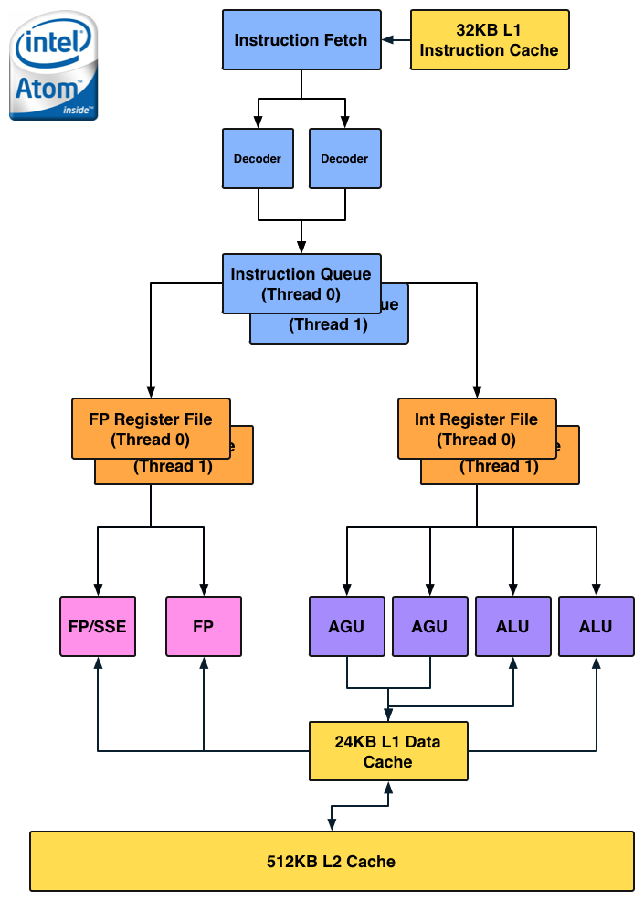
There are no dedicated integer multiply or divide units, that's all shared with the FP hardware. Intel duplicated some resources (e.g. register files, queues) to enable Hyper Threading support, but stopped short of increasing execution hardware to drive up efficiency. The tradeoff seems to have worked because Intel is able to deliver performance better than a dual-core Cortex A9 from a single HT enabled core. Intel also lucks out because while Android is very well threaded, not all tasks will continually peg both cores in a dual-core A9 machine. At higher clock speeds (1.5GHz+) and with heavy multi-threaded workloads, it's possible that a dual-core Cortex A9 could outperform (or at least equal) Medfield but I don't believe that's a realistic scenario.
Architecturally the Cortex A9 doesn't look very different from Atom:
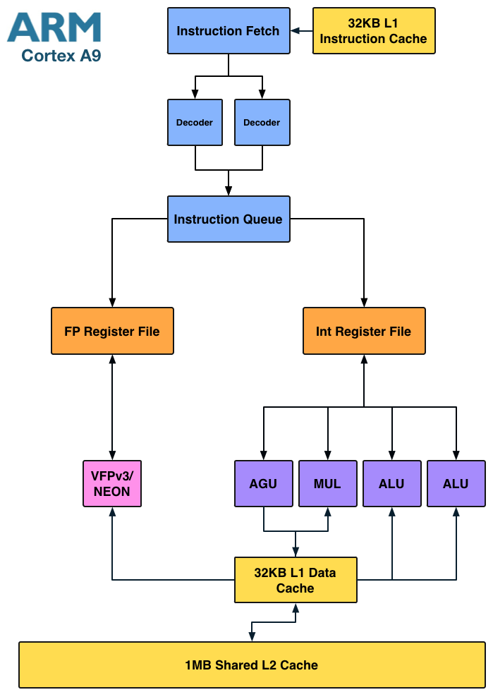
Here we see a dedicated integer multiply unit (shared with one of the ALU ports) but only a single port for FP/NEON. It's clear that the difference between Atom and the Cortex A9 isn't as obvious at the high level. Instead it's the lower level architectural decisions that gives Intel a performance advantage.
Where Intel is in trouble is if you look at the Cortex A15:
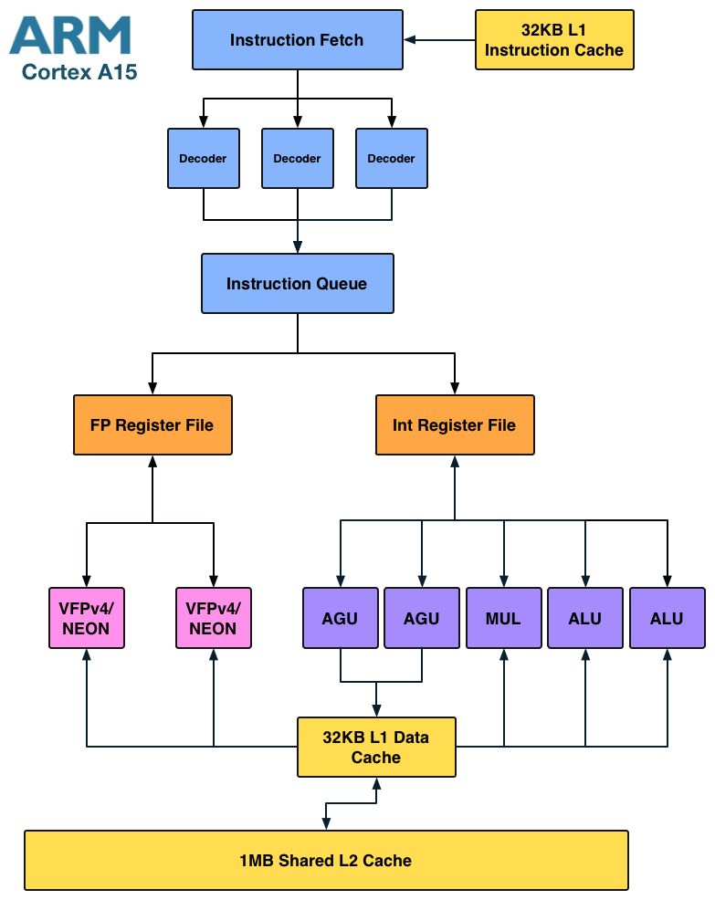
The A15 is a far more modern design, also out of order but much wider than A9. I fully expect that something A15-class can outperform Medfield, especially if the former is in a dual-core configuration. Krait falls under the A15-class umbrella so I believe Medfield has the potential to lose its CPU performance advantage within a couple of quarters.
Enhancements in Saltwell
Although the CPU core is mated to a 512KB L2 cache, there's a separate 256KB low power SRAM that runs on its own voltage plane. This ULP SRAM holds CPU state and data from the L2 cache when the CPU is power gated in the deepest sleep state. The reasoning for the separate voltage plane is simple. Intel's architects found that the minimum voltage for the core was limited by Vmin for the ULP SRAM. By putting the two on separate voltage planes it allowed Intel to bring the CPU core down to a lower minimum power state as Vmin for the L2 is higher than it is for the CPU core itself. The downside to multiple power islands is an increase in die area. Since Medfield is built on Intel's 32nm LP process while the company transitions to 22nm, spending a little more on die area to build more power efficient SoCs isn't such a big deal. Furthermore, Intel is used to building much larger chips, making Medfield's size a relative nonissue for the company.
The die size is actually very telling as it's a larger SoC than a Tegra 2 with two Cortex A9s despite only featuring a single core. Granted the rest of the blocks around the core are different, but it goes to show you that the CPU core itself (or number of cores) isn't the only determination of the die size of an SoC.
The performance tweaks come from the usual learnings that take place over the course of any architecture's lifespan. Some instruction scheduling restrictions have been lifted, memory copy performance is up, branch predictor size increased and some microcode flows run faster on Saltwell now.
Clock Speeds & Turbo
Medfield's CPU core supports several different operating frequencies and power modes. At the lowest level is its C6 state. Here the core and L2 cache are both power gated with their state is saved off in a lower power on-die SRAM. Total power consumption in C6 of the processor island is effectively zero. This isn't anything new, Intel has implemented similar technologies in desktops since 2008 (Nehalem) and notebooks since 2010 (Arrandale).
When the CPU is actually awake and doing something however it has a range of available frequencies: 100MHz all the way up to 1.6GHz in 100MHz increments.
The 1.6GHz state is a burst state and shouldn't be sustained for long periods of time, similar to how Turbo Boost works on Sandy Bridge desktop/notebook CPUs. The default maximum clock speed is 1.3GHz, although just as is the case with Turbo enabled desktop chips, you can expect to see frequencies greater than 1.3GHz on a fairly regular basis.
Power consumption along the curve is all very reasonable:
| Medfield CPU Frequency vs. Power | ||||||
| 100MHz | 600MHz | 1.3GHz | 1.6GHz | |||
| SoC Power Consumption | ~50mW | ~175mW | ~500mW | ~750mW | ||
Since most ARM based SoCs draw somewhere below 1W under full load, these numbers seem to put Medfield in line with its ARM competitors - at least on the CPU side.
It's important to pay attention to the fact that we're dealing with similar clock frequencies to what other Cortex A9 vendors are currently shipping. Any performance advantages will either be due to Medfield boosting up to 1.6GHz for short periods of time, inherently higher IPC and/or a superior cache/memory interface.


164 Comments
View All Comments
BSMonitor - Wednesday, January 11, 2012 - link
Lot of "if's" and "shoulds" in your argument.Lucian Armasu - Wednesday, January 11, 2012 - link
Well, he's comparing Atom with ARM based on benchmarks that Intel has provided, and for a chip that won't be out until the end of the year. So that's not very realistic either. Intel has been saying for a long time that "this is finally the year we're going to compete with ARM". I'm very skeptical at this point, until I really see it in the market, in a real phone, and see how it does against the competition then.tipoo - Thursday, January 12, 2012 - link
Indeed, we'll have to wait and see. Also, since this chip is a single core its easier to get its full potential, on apps that are well threaded we might see even current ARM chips beat it.Donnie Darko - Wednesday, January 11, 2012 - link
I'm generally more excited to see x86 in the market because it will drive competition more than it will drive Intel into a new field.It was an impressive technology demo, but to be honest untill they can integrate the base band radio onto the SOC they won't compete. You will be able to buy their phones and that's nice, but Qualcom will still dominate the market with Sammy/Ti and even Nvidia (shudder) rounding out most of the other designs.
Having a top to bottom stack will be nice though for everyone. Arm laptops/tablets, file servers, massivly-wide simple-instruction servers and phones. x86 HP computing (Sever->Tablets) and phones. If Intel can make enough of a beac h head then we should see AMD in the mobile space in a couple of years two. Their synthesisable CPU cores with Bobcat and their GPUs would be wicked down there.
guilmon19 - Wednesday, January 11, 2012 - link
I usually like competition as well, but when intel jumps in there i (shudder). At the moment Samsung, Motorla, qualcom, texas, ect were competing with each other with their own SoC, but they had to use the same fab to build their CPU's, but intel has their own fab(that is alot better then the ones used to build ARM) so they get a huge advantage over all those companies.Griswold - Wednesday, January 11, 2012 - link
It's the answer to a question nobody asked!tipoo - Thursday, January 12, 2012 - link
And to the left of it! Its the comment that means no one but the original poster, if even that!pugster - Wednesday, January 11, 2012 - link
Frankly, I don't know how does Intel can do 1.6ghz cpu and 400mhz gpu for less power than an arm cpu. Gees, we have seen 1.6ghz atom cpus in netbooks and the power envelope is much higher and a 32nm process can't reduce this much further.Second, the phone's cpu is usually in deep sleep most of the time, intel didn't really benchmark what happens when the phone is idle, IE standby time.
Third, is cost. Unless Intel start selling these cpus at giveaway prices for less than $15, I doubt that these phones are competitive to ARM variants.
Fourth is adoption rate. Considering that most of the apps are written for the ARM cpus, I wonder when phone manufacturers and porogrammers will port intel version of their apps.
bobsmith1492 - Thursday, January 12, 2012 - link
The article covers power consumption and porting.Cost is a valid concern! Real-life use cycles will be good to show how quick it transitions into and out of sleep for real-life power use. Being faster when active with the same power use though it should be better if anything. The clock rate scaling will compete against the big-little architecture for ARM, too.
Roy2001 - Wednesday, January 11, 2012 - link
Very impressive. Good job Intel!