AMD Radeon HD 7970 Review: 28nm And Graphics Core Next, Together As One
by Ryan Smith on December 22, 2011 12:00 AM EST- Posted in
- GPUs
- AMD
- Radeon
- ATI
- Radeon HD 7000
Theoreticals & Tessellation
From a rendering perspective one of the most interesting things AMD did with Tahiti was what they didn’t do: they didn’t add more ROPs, they didn’t add more geometry engines. And yet based on our game performance they’ve clearly improved on their performance in those situations by making more efficient use of the hardware they do have.
So we wanted to take a quick look at synthetic performance to see what these tools had to say about AMD’s changes. We’ve included the numbers for every other GPU in our lineup as a reference point, but we would strongly suggest against reading into them too much. AMD versus AMD is sometimes relevant to real world performance; AMD versus NVIDIA rarely is.
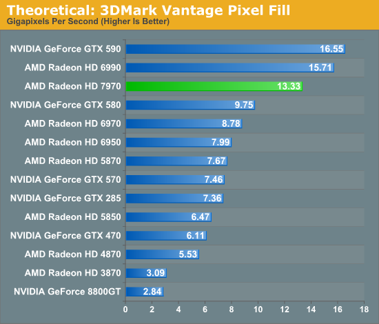
We’ll start with 3DMark Vantage and its color fill test. This is basically a ROP test that attempts to have a GPU’s ROPs blend as many pixels as it can. Theoretically AMD can do 32 color operations per clock on Tahiti, which at 925MHz for 7970 means the theoretical limit is 29.6Gpix/sec; not that any architecture is ever that efficient. In practice 7970 hits 13.33Gpix/sec, which is still well short of the theoretical maximum, but pay close attention to 7970’s performance relative to 6970. Even with the same number of ROPs and a similar theoretical performance limit (29.6 vs 28.16), 7970 is pushing 51% more pixels than 6970 is.
In designing Tahiti AMD said that they didn’t need more ROPs they just needed more efficient ROPs, and it looks like they’ve delivered on this. It’s not clear whether this is the limit for efficiency or if AMD can squeeze more out of their ROPs in future designs, but this definitely helps to prove that there’s more to graphics rendering than a large number of functional units.
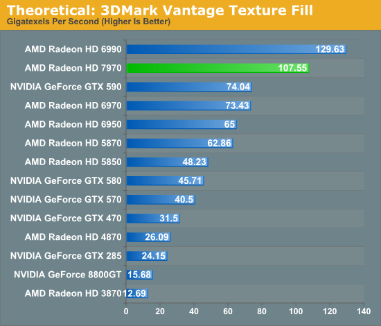
Our other 3DMark synthetic benchmark is the 3DMark Vantage Texture Blend test, which measures how quickly a GPU can blend multiple FP16 textures. This is more synthetic than most tests because FP16 textures aren’t widely used, but it’s a consistent benchmark.
The theoretical performance improvement from 6970 to 7970 is 40% - 33% more texture units operating at a 5% higher clockspeed. In practice the 7970 exceeds that improvement by increasing texture performance by 46%, meaning the 7970 has benefitted from more than the increase in texture units. Most likely the new cache architecture has further improved the efficiency of the texture units, although the 3DMark texture set is not particularly large.
Moving on, we also wanted to take a look at tessellation. AMD did not increase the theoretical geometry performance of Tahiti as compared to Cayman – both top out at 2 triangles per clock – but AMD has put a lot of effort into improving the efficiency of Tahiti’s geometry units as we’ve seen reflected in our game benchmarks.
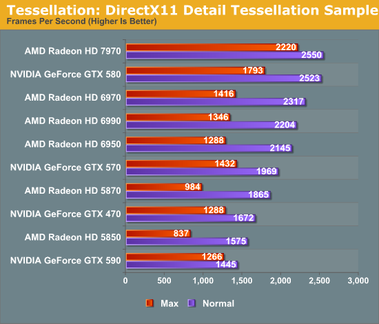
Our first tessellation benchmark is the traditional Detail Tessellation sample program from the DirectX SDK. Here we’re looking at tessellation performance as a product of the framerate, testing at tessellation factors 7 (normal) and 15 (max). Traditionally this is a test that has been rather balanced at normal tessellation levels, while NVIDIA cards with their superior geometry throughput have been the top performers at maximum tessellation levels. So it’s all the more interesting when we’ve seen the tables turned; the 7970 is merely competitive with the GTX 580 at normal tessellation levels, but now it’s ahead of the GTX 580 by 24%. More significantly however the 7970 is ahead of the 6970 by 57%.
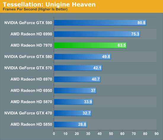
Our second tessellation benchmark is Unigine Heaven, a benchmark that straddles the line between a synthetic benchmark and a real-world benchmark, as the engine is licensed but no notable DX11 games have been produced using it yet. In any case the Heaven benchmark is notable for its heavy use of tessellation, which means it’s largely a proxy test for tessellation performance.
As with the Detail Tessellation sample program, Heaven shows significant gains for the 7970 versus the 6970, with the 7970 leading by 56%. Meanwhile it leads the GTX 580 by 27%, which is actually slightly better than what we saw under the more “pure” Detail Tessellation sample. Between these two benchmarks it’s clear that AMD’s tessellation efficiency improvements are quite real, and that with Tahiti AMD can deliver much better tessellation performance than Cayman even at virtually the same theoretical triangle throughput rate.
Of course one has to wonder what NVIDIA will have in store for Kepler next year. Their current Fermi design seems to scale well with additional geometry units, but if Tahiti is anything to go by, there’s a great deal to be gained just by focusing on efficiency. NVIDIA has prided themselves on their geometry performance since before GF100 even shipped, so it will be interesting if they have anything in store to hold on to that distinction.


292 Comments
View All Comments
GTVic - Thursday, December 22, 2011 - link
The first Fermi version they demo'd was a mock-up held together with wood screws. That is not a good launch...RussianSensation - Thursday, December 22, 2011 - link
And the real launch version produced Tessellation performance that took HD7970 to pass, had compute performance that HD7970 can barely best today, had Mega Texture support that HD7970 just added now 2 years later, had scalar SIMD architecture that took AMD 2 years to release.Scali - Friday, December 23, 2011 - link
HD7970 doesn't actually surpass Fermi's tessellation, apart from tessellation factors 10 and below:http://www.pcgameshardware.de/aid,860536/Test-Rade...
From factor 11 to 64, Fermi still reigns supreme.
(This is with AMD's SubD11 sample from the DirectX 11 SDK).
Scali - Friday, December 23, 2011 - link
Uhhh no. They demo'ed a real Fermi obviously.It was just a development board, which didn't exactly look pretty, and was not in any way representative of the card that would be available to end-users.
So they made a mock-up to show what a retail Fermi WOULD look like, once it hits the stores.
Which is common practice anyway in the industry.
fllib19554 - Thursday, January 12, 2012 - link
off yourself cretin.futurepastnow - Thursday, December 22, 2011 - link
You misspelled "impressive."slayernine - Thursday, December 22, 2011 - link
What Wreckage really meant to say was that it was disappointing for nVidia to get pummelled so thoroughly.unaligned - Friday, December 23, 2011 - link
A year old card pummeled by the newest technology? I would hope so.MagickMan - Thursday, December 22, 2011 - link
Go shoot yourself in the face, troll.rs2 - Thursday, December 22, 2011 - link
Yes, yes. 4+ billion transistors on a single chip is not impressive at all. Why, it's not even one transistor for every person on the planet yet.