AMD Radeon HD 7970 Review: 28nm And Graphics Core Next, Together As One
by Ryan Smith on December 22, 2011 12:00 AM EST- Posted in
- GPUs
- AMD
- Radeon
- ATI
- Radeon HD 7000
A Quick Refresher: Graphics Core Next
One of the things we’ve seen as a result of the shift from pure graphics GPUs to mixed graphics and compute GPUs is how NVIDIA and AMD go about making their announcements and courting developers. With graphics GPUs there was no great need to discuss products or architectures ahead of time; a few choice developers would get engineering sample hardware a few months early, and everyone else would wait for the actual product launch. With the inclusion of compute capabilities however comes the need to approach launches in a different manner, a more CPU-like manner.
As a result both NVIDIA and AMD have begun revealing their architectures to developers roughly six months before the first products launch. This is very similar to how CPU launches are handled, where the basic principles of an architecture are publically disclosed months in advance. All of this is necessary as the compute (and specifically, HPC) development pipeline is far more focused on optimizing code around a specific architecture in order to maximize performance; whereas graphics development is still fairly abstracted by APIs, compute developers want to get down and dirty, and to do that they need to know as much about new architectures as possible as soon as possible.
It’s for these reasons that AMD announced Graphics Core Next, the fundamental architecture behind AMD’s new GPUs, back in June of this year at the AMD Fusion Developers Summit. There are some implementation and product specific details that we haven’t known until now, and of course very little was revealed about GCN’s graphics capabilities, but otherwise on the compute side AMD is delivering on exactly what they promised 6 months ago.
Since we’ve already covered the fundamentals of GCN in our GCN preview and the Radeon HD 7970 is primarily a gaming product we’re not going to go over GCN in depth here, but I’d encourage you to read our preview to fully understand the intricacies of GCN. But if you’re not interested in that, here’s a quick refresher on GCN with details pertinent to the 7970.
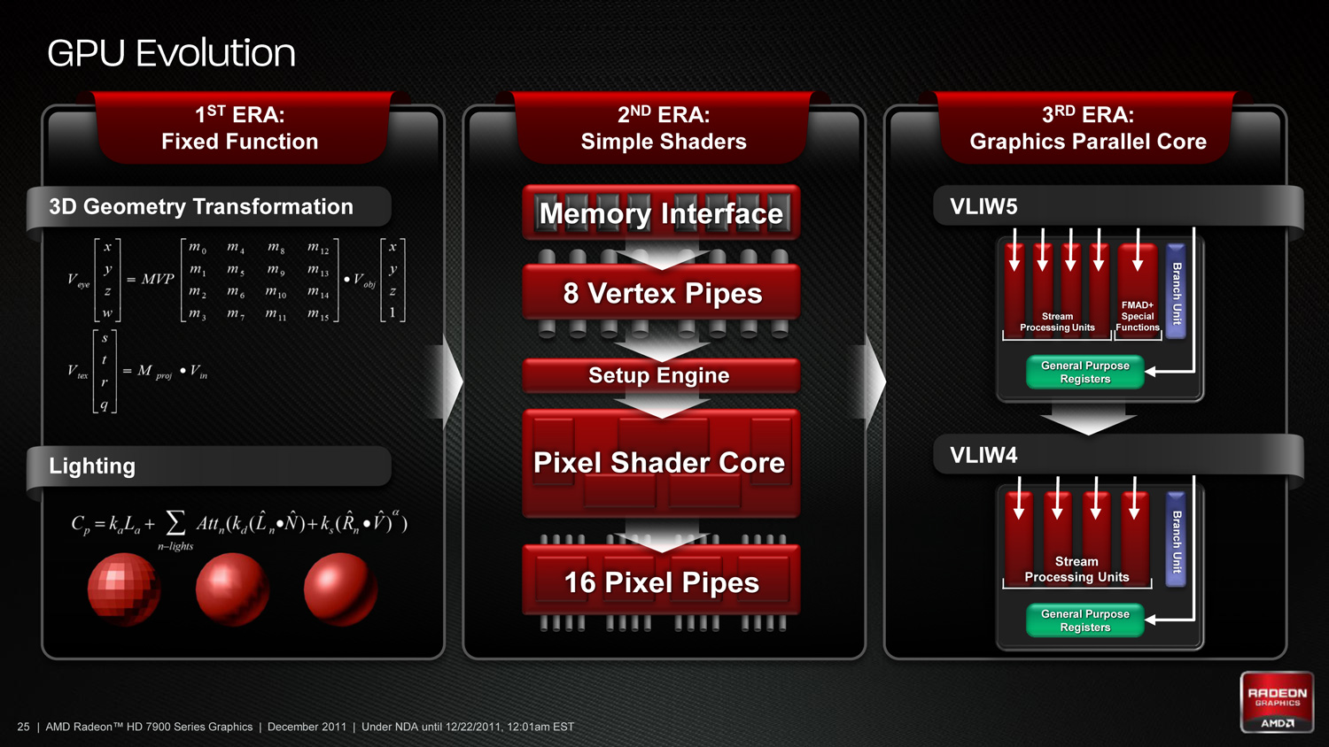
As we’ve already seen in some depth with the Radeon HD 6970, VLIW architectures are very good for graphics work, but they’re poor for compute work. VLIW designs excel in high instruction level parallelism (ILP) use cases, which graphics falls under quite nicely thanks to the fact that with most operations pixels and the color component channels of pixels are independently addressable datum. In fact at the time of the Cayman launch AMD found that the average slot utilization factor for shader programs on their VLIW5 architecture was 3.4 out of 5, reflecting the fact that most shader operations were operating on pixels or other data types that could be scheduled together
Meanwhile, at a hardware level VLIW is a unique design in that it’s the epitome of the “more is better” philosophy. AMD’s high steam processor counts with VLIW4 and VLIW5 are a result of VLIW being a very thin type of architecture that purposely uses many simple ALUs, as opposed to fewer complex units (e.g. Fermi). Furthermore all of the scheduling for VLIW is done in advance by the compiler, so VLIW designs are in effect very dense collections of simple ALUs and cache.
The hardware traits of VLIW mean that for a VLIW architecture to work, the workloads need to map well to the architecture. Complex operations that the simple ALUs can’t handle are bad for VLIW, as are instructions that aren’t trivial to schedule together due to dependencies or other conflicts. As we’ve seen graphics operations do map well to VLIW, which is why VLIW has been in use since the earliest pixel shader equipped GPUs. Yet even then graphics operations don’t achieve perfect utilization under VLIW, but that’s okay because VLIW designs are so dense that it’s not a big problem if they’re operating at under full efficiency.
When it comes to compute workloads however, the idiosyncrasies of VLIW start to become a problem. “Compute” covers a wide range of workloads and algorithms; graphics algorithms may be rigidly defined, but compute workloads can be virtually anything. On the one hand there are compute workloads such as password hashing that are every bit as embarrassingly parallel as graphics workloads are, meaning these map well to existing VLIW architectures. On the other hand there are tasks like texture decompression which are parallel but not embarrassingly so, which means they map poorly to VLIW architectures. At one extreme you have a highly parallel workload, and at the other you have an almost serial workload.
Cayman, A VLIW4 Design
So long as you only want to handle the highly parallel workloads VLIW is fine. But using VLIW as the basis of a compute architecture is going is limit what tasks your processor is sufficiently good at. If you want to handle a wider spectrum of compute workloads you need a more general purpose architecture, and this is the situation AMD faced.
But why does AMD want to chase compute in the first place when they already have a successful graphics GPU business? In the long term GCN plays a big part in AMD’s Fusion plans, but in the short term there’s a much simpler answer: because they have to.
In Q3’2011 NVIDIA’s Professional Solutions Business (Quadro + Tesla) had an operating income of 95M on 230M in revenue. Their (consumer) GPU business had an operating income of 146M, but on a much larger 644M in revenue. Professional products have much higher profit margins and it’s a growing business, particularly the GPU computing side. As it stands NVIDIA and AMD may have relatively equal shares of the discrete GPU market, but it’s NVIDIA that makes all the money. For AMD’s GPU business it’s no longer enough to focus only on graphics, they need a larger piece of the professional product market to survive and thrive in the future. And thus we have GCN.


292 Comments
View All Comments
GTVic - Thursday, December 22, 2011 - link
The first Fermi version they demo'd was a mock-up held together with wood screws. That is not a good launch...RussianSensation - Thursday, December 22, 2011 - link
And the real launch version produced Tessellation performance that took HD7970 to pass, had compute performance that HD7970 can barely best today, had Mega Texture support that HD7970 just added now 2 years later, had scalar SIMD architecture that took AMD 2 years to release.Scali - Friday, December 23, 2011 - link
HD7970 doesn't actually surpass Fermi's tessellation, apart from tessellation factors 10 and below:http://www.pcgameshardware.de/aid,860536/Test-Rade...
From factor 11 to 64, Fermi still reigns supreme.
(This is with AMD's SubD11 sample from the DirectX 11 SDK).
Scali - Friday, December 23, 2011 - link
Uhhh no. They demo'ed a real Fermi obviously.It was just a development board, which didn't exactly look pretty, and was not in any way representative of the card that would be available to end-users.
So they made a mock-up to show what a retail Fermi WOULD look like, once it hits the stores.
Which is common practice anyway in the industry.
fllib19554 - Thursday, January 12, 2012 - link
off yourself cretin.futurepastnow - Thursday, December 22, 2011 - link
You misspelled "impressive."slayernine - Thursday, December 22, 2011 - link
What Wreckage really meant to say was that it was disappointing for nVidia to get pummelled so thoroughly.unaligned - Friday, December 23, 2011 - link
A year old card pummeled by the newest technology? I would hope so.MagickMan - Thursday, December 22, 2011 - link
Go shoot yourself in the face, troll.rs2 - Thursday, December 22, 2011 - link
Yes, yes. 4+ billion transistors on a single chip is not impressive at all. Why, it's not even one transistor for every person on the planet yet.