AMD Radeon HD 7970 Review: 28nm And Graphics Core Next, Together As One
by Ryan Smith on December 22, 2011 12:00 AM EST- Posted in
- GPUs
- AMD
- Radeon
- ATI
- Radeon HD 7000
A Quick Refresher: Graphics Core Next
One of the things we’ve seen as a result of the shift from pure graphics GPUs to mixed graphics and compute GPUs is how NVIDIA and AMD go about making their announcements and courting developers. With graphics GPUs there was no great need to discuss products or architectures ahead of time; a few choice developers would get engineering sample hardware a few months early, and everyone else would wait for the actual product launch. With the inclusion of compute capabilities however comes the need to approach launches in a different manner, a more CPU-like manner.
As a result both NVIDIA and AMD have begun revealing their architectures to developers roughly six months before the first products launch. This is very similar to how CPU launches are handled, where the basic principles of an architecture are publically disclosed months in advance. All of this is necessary as the compute (and specifically, HPC) development pipeline is far more focused on optimizing code around a specific architecture in order to maximize performance; whereas graphics development is still fairly abstracted by APIs, compute developers want to get down and dirty, and to do that they need to know as much about new architectures as possible as soon as possible.
It’s for these reasons that AMD announced Graphics Core Next, the fundamental architecture behind AMD’s new GPUs, back in June of this year at the AMD Fusion Developers Summit. There are some implementation and product specific details that we haven’t known until now, and of course very little was revealed about GCN’s graphics capabilities, but otherwise on the compute side AMD is delivering on exactly what they promised 6 months ago.
Since we’ve already covered the fundamentals of GCN in our GCN preview and the Radeon HD 7970 is primarily a gaming product we’re not going to go over GCN in depth here, but I’d encourage you to read our preview to fully understand the intricacies of GCN. But if you’re not interested in that, here’s a quick refresher on GCN with details pertinent to the 7970.
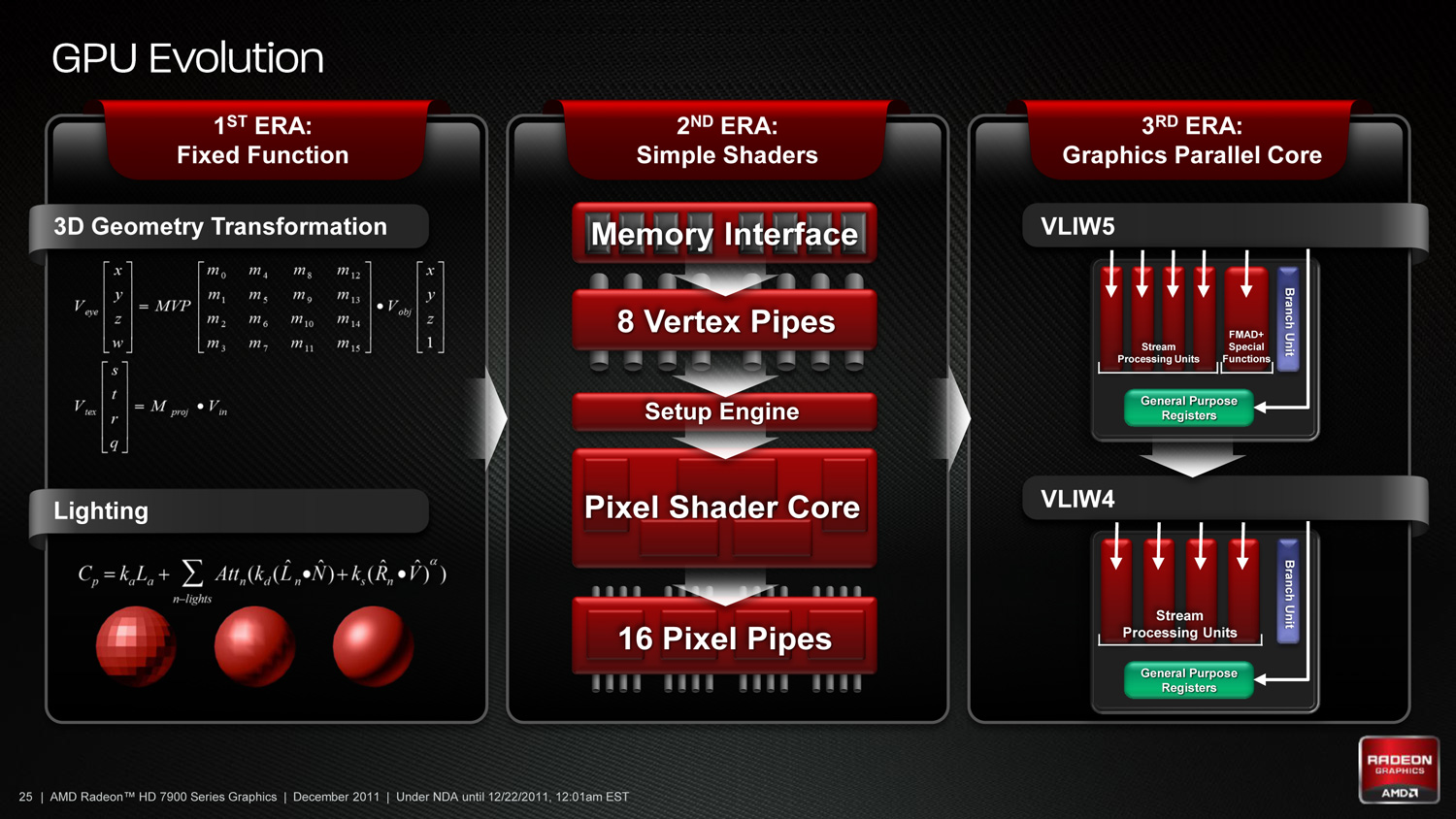
As we’ve already seen in some depth with the Radeon HD 6970, VLIW architectures are very good for graphics work, but they’re poor for compute work. VLIW designs excel in high instruction level parallelism (ILP) use cases, which graphics falls under quite nicely thanks to the fact that with most operations pixels and the color component channels of pixels are independently addressable datum. In fact at the time of the Cayman launch AMD found that the average slot utilization factor for shader programs on their VLIW5 architecture was 3.4 out of 5, reflecting the fact that most shader operations were operating on pixels or other data types that could be scheduled together
Meanwhile, at a hardware level VLIW is a unique design in that it’s the epitome of the “more is better” philosophy. AMD’s high steam processor counts with VLIW4 and VLIW5 are a result of VLIW being a very thin type of architecture that purposely uses many simple ALUs, as opposed to fewer complex units (e.g. Fermi). Furthermore all of the scheduling for VLIW is done in advance by the compiler, so VLIW designs are in effect very dense collections of simple ALUs and cache.
The hardware traits of VLIW mean that for a VLIW architecture to work, the workloads need to map well to the architecture. Complex operations that the simple ALUs can’t handle are bad for VLIW, as are instructions that aren’t trivial to schedule together due to dependencies or other conflicts. As we’ve seen graphics operations do map well to VLIW, which is why VLIW has been in use since the earliest pixel shader equipped GPUs. Yet even then graphics operations don’t achieve perfect utilization under VLIW, but that’s okay because VLIW designs are so dense that it’s not a big problem if they’re operating at under full efficiency.
When it comes to compute workloads however, the idiosyncrasies of VLIW start to become a problem. “Compute” covers a wide range of workloads and algorithms; graphics algorithms may be rigidly defined, but compute workloads can be virtually anything. On the one hand there are compute workloads such as password hashing that are every bit as embarrassingly parallel as graphics workloads are, meaning these map well to existing VLIW architectures. On the other hand there are tasks like texture decompression which are parallel but not embarrassingly so, which means they map poorly to VLIW architectures. At one extreme you have a highly parallel workload, and at the other you have an almost serial workload.
Cayman, A VLIW4 Design
So long as you only want to handle the highly parallel workloads VLIW is fine. But using VLIW as the basis of a compute architecture is going is limit what tasks your processor is sufficiently good at. If you want to handle a wider spectrum of compute workloads you need a more general purpose architecture, and this is the situation AMD faced.
But why does AMD want to chase compute in the first place when they already have a successful graphics GPU business? In the long term GCN plays a big part in AMD’s Fusion plans, but in the short term there’s a much simpler answer: because they have to.
In Q3’2011 NVIDIA’s Professional Solutions Business (Quadro + Tesla) had an operating income of 95M on 230M in revenue. Their (consumer) GPU business had an operating income of 146M, but on a much larger 644M in revenue. Professional products have much higher profit margins and it’s a growing business, particularly the GPU computing side. As it stands NVIDIA and AMD may have relatively equal shares of the discrete GPU market, but it’s NVIDIA that makes all the money. For AMD’s GPU business it’s no longer enough to focus only on graphics, they need a larger piece of the professional product market to survive and thrive in the future. And thus we have GCN.


292 Comments
View All Comments
Ryan Smith - Thursday, December 22, 2011 - link
Since 1920x1200 has already been commented on elsewhere I'm just going to jump right to your comment on minimum FPS.I completely agree, and we're trying to add it where it makes sense. A lot of benchmarks are wildly inconsistent about their minimum FPS, largely thanks to the fact that minimum FPS is an instantaneous data point. When your values vary by 20%+ per run (as minimums often do), even averaging repeated trials isn't nearly accurate enough to present meaningful results.
CeriseCogburn - Thursday, March 8, 2012 - link
HardOCP shows long in game fps per second charts that show dips and bottom outs are more than one momentary lapse and often are extended time periods of lowest frame rate runs, so I have to respectfully disagree.Perhaps the fault is fraps can show you a single instance of lowest frame rate number, and hence it's the analysis that utterly fails - given the time constraints that were made obvious, it is also clear that the extra work it would take for an easily reasoned and reasonable result that is actually of worthy accuracy is not in the cards here.
thunderising - Thursday, December 22, 2011 - link
Okay. This card has left me thrilled, but wanting for more. Why?Well, for example, every reviewer has hit the CCC Core and Memory Max Limits, which turns into a healthy 10-12% performance boost, all for 10W.
What, legit reviews got it to 1165MHz core and 6550Mhz memory for a 21-24% increase in performance. Now that's HUGE!
I think AMD could have gone for something like this with the final clocks, to squeeze out every last bit of performance from this amazing card:
Core - 1050 MHz
Memory - 1500 MHz (6000MHz QDR)
This was not only easily achievable, but would have placed this card at a 8-10% increase in performance all for a mere <10W rise in Load Power.
Hoping for AIBs like Sapphire to show their magic! HD7970 Toxic, MmmmmmM...
Otherwise, fantastic card I say.
Death666Angel - Friday, December 23, 2011 - link
Maybe they'll do a 4870/4890 thing again? Launch the HD7970 and HD7970X2 and then launch a HD7990 with higher clocks later to counter nVidia.... Who knows. :-)Mishera - Sunday, December 25, 2011 - link
They've been doing it for quite some time now. Their plan has been to release a chip balancing die size, performance, and cost. Then later to compete on high end release a dual-chip card. Anand wrote on this a while ago with the rv770 story (http://www.anandtech.com/show/2679).Even looking at the picture of chip sizes, the 7970 is still a reasonable size. And this really was a brilliant move as though Nvidia has half the marketshare and does make a lot of money from their cards, their design philosophy has been hurting them a lot from a business standpoint.
On a side note, Amd really made a great choice by choosing to wait until now to push for general computing. Though that probably means more people to support development and drivers, which means more hiring which is the opposite way Amd has been going. It will be interesting to see how this dichotomy will develop in the future. But right now kudos to Amd.
CeriseCogburn - Thursday, March 8, 2012 - link
Does that mean amd is abandoning gamers as we heard the scream whilst Nvidia was doing thus ?I don't quite get it - now what nvidia did that hurt them, is praise worthy since amd did it, finally.
Forgive me as I scoff at the immense dichotomy...
"Perfect ripeness at the perfect time" - sorry not buying it....
privatosan - Thursday, December 22, 2011 - link
PRT is a nice feature, but there is an failure in the article:'For AMD’s technology each tile will be 64KB, which for an uncompressed 32bit texture would be enough room for a 4K x 4K chunk.'
The tile would be 128 x 128 texels; 4K x 4K would be quite big for a tile.
futrtrubl - Thursday, December 22, 2011 - link
I was going to comment on that too. A 4k x 4k x 32bit (4byte) texture chunk would be around 67MB uncompressed. For a 32bit texture you could only fit a 128x128 array in a 64KB chunk. An 8bit/pixel texture could be 4k*4kStonedofmoo - Thursday, December 22, 2011 - link
Thanks for the review. A request though...To the hardware sites doing these reviews, many of us in this day and age run dual monitor or more. It always frustrates in me in these reviews that we get a long write up on the power saving techniques the new cards use, and never any mention of it helps those of us running more than one display.
For those not in the know, if you run more than one display on all the current generations the cards do NOT downclock the GPU and memory nearly as much as they do on single montor configurations. This burns quite a lot more power and obviously kicks out more heat. No site ever mentions this which is odd considering so many of us have more than one display these days.
I would happily buy the card that finally overcomes this and actually finds a way of knocking back the clocks with multi-monitor setups. Is the new Radeon 7xxx series that card?
Galcobar - Thursday, December 22, 2011 - link
It's in the article, on the page entitled "Meet the Radeon 7970."Ryan also replied to a similar comment by quoting the paragraph addressing multi-monitor setups and power consumption at the top of page of the comments.
That's two mentions, and the answer to your question.