Intel Core i7 3960X (Sandy Bridge E) Review: Keeping the High End Alive
by Anand Lal Shimpi on November 14, 2011 3:01 AM EST- Posted in
- CPUs
- Intel
- Core i7
- Sandy Bridge
- Sandy Bridge E
If you look carefully enough, you may notice that things are changing. It first became apparent shortly after the release of Nehalem. Intel bifurcated the performance desktop space by embracing a two-socket strategy, something we'd never seen from Intel and only once from AMD in the early Athlon 64 days (Socket-940 and Socket-754).
LGA-1366 came first, but by the time LGA-1156 arrived a year later it no longer made sense to recommend Intel's high-end Nehalem platform. Lynnfield was nearly as fast and the entire platform was more affordable.
When Sandy Bridge launched earlier this year, all we got was the mainstream desktop version. No one complained because it was fast enough, but we all knew an ultra high-end desktop part was in the works. A true successor to Nehalem's LGA-1366 platform for those who waited all this time.
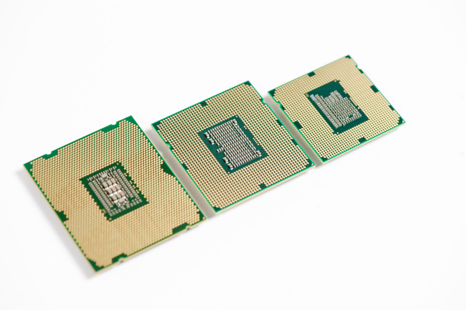
Left to right: Sandy Bridge E, Gulftown, Sandy Bridge
After some delays, Sandy Bridge E is finally here. The platform is actually pretty simple to talk about. There's a new socket: LGA-2011, a new chipset Intel's X79 and of course the Sandy Bridge E CPU itself. We'll start at the CPU.
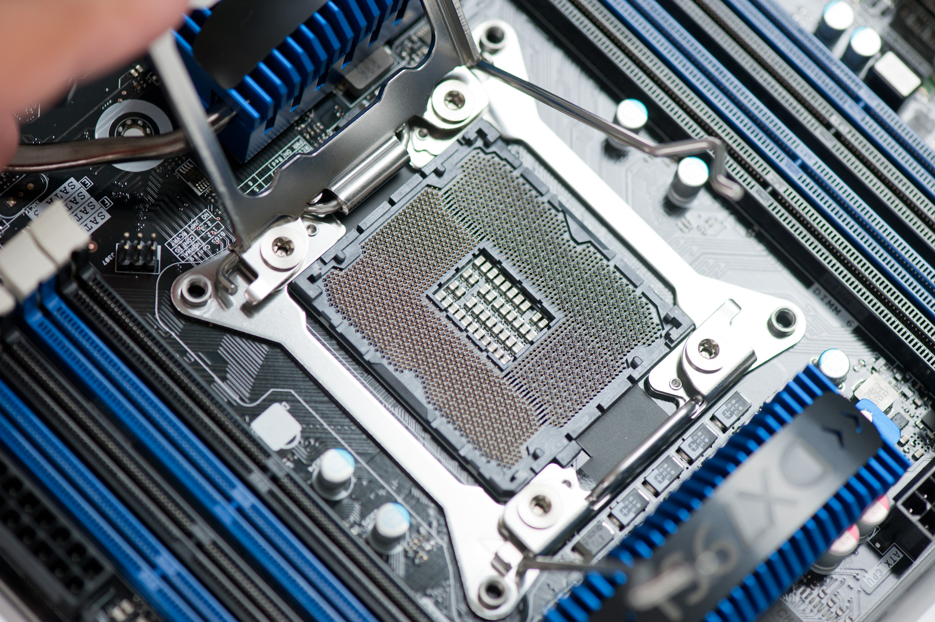
LGA-2011, the new socket
For the desktop, Sandy Bridge E is only available in 6-core configurations at launch. Early next year we'll see a quad-core version. I mention the desktop qualification because Sandy Bridge E is really a die harvested Sandy Bridge EP, Intel's next generation Xeon part:

Sandy Bridge E die
If you look carefully at the die shot above, you'll notice that there are actually eight Sandy Bridge cores. The Xeon version will have all eight enabled, but the last two are fused off for SNB-E. The 32nm die is absolutely gigantic by desktop standards, measuring 20.8 mm x 20.9 mm (~435mm^2) Sandy Bridge E is bigger than most GPUs. It also has a ridiculous number of transistors: 2.27 billion.
Around a quarter of the die is dedicated just to the chip's massive L3 cache. Each cache slice has increased in size compared to Sandy Bridge. Instead of 2MB, Sandy Bridge E boasts 2.5MB cache slices. In its Xeon configuration that works out to 20MB of L3 cache, but for desktops it's only 15MB. That's just 1MB shy of how much system memory my old upgraded 386-SX/20 had.
| CPU Specification Comparison | ||||||||
| CPU | Manufacturing Process | Cores | Transistor Count | Die Size | ||||
| AMD Bulldozer 8C | 32nm | 8 | 1.2B* | 315mm2 | ||||
| AMD Thuban 6C | 45nm | 6 | 904M | 346mm2 | ||||
| AMD Deneb 4C | 45nm | 4 | 758M | 258mm2 | ||||
| Intel Gulftown 6C | 32nm | 6 | 1.17B | 240mm2 | ||||
| Intel Sandy Bridge E (6C) | 32nm | 6 | 2.27B | 435mm2 | ||||
| Intel Nehalem/Bloomfield 4C | 45nm | 4 | 731M | 263mm2 | ||||
| Intel Sandy Bridge 4C | 32nm | 4 | 995M | 216mm2 | ||||
| Intel Lynnfield 4C | 45nm | 4 | 774M | 296mm2 | ||||
| Intel Clarkdale 2C | 32nm | 2 | 384M | 81mm2 | ||||
| Intel Sandy Bridge 2C (GT1) | 32nm | 2 | 504M | 131mm2 | ||||
| Intel Sandy Bridge 2C (GT2) | 32nm | 2 | 624M | 149mm2 | ||||
Update: AMD originally told us Bulldozer was a 2B transistor chip. It has since told us that the 8C Bulldozer is actually 1.2B transistors. The die size is still accurate at 315mm2.
At the core level, Sandy Bridge E is no different than Sandy Bridge. It doesn't clock any higher, L1/L2 caches remain unchanged and per-core performance is identical to what Intel launched earlier this year.


The Lineup
| Processor | Core Clock | Cores / Threads | L3 Cache | Max Turbo | Max Overclock Multiplier | TDP | Price |
| Intel Core i7 3960X | 3.3GHz | 6 / 12 | 15MB | 3.9GHz | 57x | 130W | $990 |
| Intel Core i7 3930K | 3.2GHz | 6 / 12 | 12MB | 3.8GHz | 57x | 130W | $555 |
| Intel Core i7 3820 | 3.6GHz | 4 / 8 | 10MB | 3.9GHz | 43x | 130W | TBD |
| Intel Core i7 2700K | 3.5GHz | 4 / 8 | 8MB | 3.9GHz | 57x | 95W | $332 |
| Intel Core i7 2600K | 3.4GHz | 4 / 8 | 8MB | 3.8GHz | 57x | 95W | $317 |
| Intel Core i7 2600 | 3.4GHz | 4 / 8 | 8MB | 3.8GHz | 42x | 95W | $294 |
| Intel Core i5 2500K | 3.3GHz | 4 / 4 | 6MB | 3.7GHz | 57x | 95W | $216 |
| Intel Core i5 2500 | 3.3GHz | 4 / 4 | 6MB | 3.7GHz | 41x | 95W | $205 |
Those of you buying today only have two options: the Core i7-3960X and the Core i7-3930K. Both have six fully unlocked cores, but the 3960X gives you a 15MB L3 cache vs. 12MB with the 3930K. You pay handsomely for that extra 3MB of L3. The 3960X goes for $990 in 1K unit quantities, while the 3930K sells for $555.
The 3960X has the same 3.9GHz max turbo frequency as the Core i7 2700K, that's with 1 - 2 cores active. With 5 - 6 cores active the max turbo drops to a respectable 3.6GHz. Unlike the old days of many vs. few core CPUs, there are no tradeoffs for performance when you buy a SNB-E. Thanks to power gating and turbo, you get pretty much the fastest possible clock speeds regardless of workload.
Early next year we'll see a Core i7 3820, priced around $300, with only 4 cores and a 10MB L3. The 3820 will only be partially unlocked (max OC multiplier = 4 bins above max turbo).


163 Comments
View All Comments
jabber - Monday, November 14, 2011 - link
...with Pixar updating their rendering farm?I cant think of many other big customers for this kind of chip.
randinspace - Monday, November 14, 2011 - link
Wouldn't they be using Xeons?gevorg - Monday, November 14, 2011 - link
Could the wasted space for 2 fused cores and their L3 cache been used for HD2000 graphics? Wish Intel would have avoided wasting die space like this.GL1zdA - Monday, November 14, 2011 - link
It's not wasting, it's binning. They could either throw away 8-cores with damaged cores or sell them as six-cores, which is what they did.BSMonitor - Monday, November 14, 2011 - link
Actually it's not binning in this case. (some chips from the Xeon line might be) But these "desktop" CPUs are actually the 8-core Xeon line trimmed down in both cost and validation for use in Desktop PCs. Intel's currently roadmap is 6-core desktop CPU's at the high-end with extremely high memory bandwidth.It is cheaper for them to fuse two cores from an 8-core Xeon production line, than to redesign another CPU die for just the high-end 6-core desktop line. This class is by no means high-volume, hence yet another CPU die would be expensive.
GL1zdA - Monday, November 14, 2011 - link
Could you test how Sandy Bridge-E behaves in vt_benchmark when GPU trancoding is used? I'm curious, if SBE will do better than a nVidia 580. And what is the difference between 2600K+580 and 3960X+580 when GPU transcoding is enabled.Kevin G - Monday, November 14, 2011 - link
Intel crippled both the CPU and the chipset with this launch. I was hoping to see an 8 core model at the high end. The chip design itself is an 8 core die so why not a fully functional chip for the low volume extreme edition? The performance benefits of the Core i7 3960X over the 990X mirror those from the 2600K over the 875K. (Well actually the 2600K vs. 875K comparison is much wider due to the clock speed differences, not just the architectural changes.) Sure it is faster at stock but generally not worth upgrading to, especially factoring in motherboard cost. Another let down is that the chip doesn't officially support PCI-E 3.0 True that their are no PCI-E 3.0 cards on the market today but there will be tomorrow. Not sure if this is additional crippling to distinguish the consumer chips from the coming LGA2011 Xeons or if there actually was a problem running at PCI-E 3.0 speeds.Speaking of Xeons, this article didn't mention if the system has the two QPI links disabled. If not, there could be the remote chance of a manufacturer releasing a board with the X79 using DMI and an X58 chipset hanging off of a QPI link. That would allow for another two full bandwidth PCI-E 16X slots at 2.0 speeds without the usage of a bridge chip.
Then there is the X79 chipset. The reality is that it offers very little over the Z68. No USB 3.0 or additional SATA ports are the big things. Knowing Intel, we'll likely see a Z79 chipset that'll enable the SAS functionality for those that want more storage. Hopefully the hypothetical Z79 chipset will also use some of the PCI-E lanes from the CPU for additional bandwidth as an array of SSD's would easily be able to saturate the current DMI link.
I'm also curious if these X79 consumer boards will allow for some overclocking with an LGA 2011 Xeon. I'm not expected full multiplier controller but rather feeding that 125 Mhz or 166 Mhz base clock to the CPU would suffice. Getting one of these consumer boards and paying the Xeon premium may wind up being the way to go for a true leap over of the Core i7 990X.
khanov - Monday, November 14, 2011 - link
This is a good question, I guess many would wonder why this is the case. To understand why requires a little insight into the manufacturing of silicon chips:
As with almost any manufacturing process there are variables that differentiate one product coming off the same assembly line from the next. So for example at a car factory each 'identical' engine is in fact a little different from another, whether it be the balancing of the crankshaft or the exact fit of the bearings.
With the manufacturing of CPUs (and indeed any silicon chips) there are also small differences between the chips that come off the same assembly line. If a chip has a defect for example (which happens too frequently) the defective area of the chip needs to be disabled. In essence this is why we are seeing Sandy Bridge-E cpus launching with disabled cores.
The fully enabled cores (eight cores and 20MB L3 cache) are being sold as (or will soon be sold as) Xeon chips for the highest price. Somewhat lesser cores with defects are being sold as lower end Xeons with six cores or as consumer Sandy Bridge-E chips with six cores. Even more defective chips that can only work with four cores enabled are being stockpiled and will soon be sold as four core Sandy-Bridge-E and Xeon chips.
So basically all these chips are manufactured with eight 'possible' cores. There is no wasted space on the die. However due to imperfect manufacturing processes some of these chips will have defects. In fact the larger the die area the more likely a defect occurs within each chip. With a very large die area for SB-E intel is now experiencing a problem more often seen by GPU manufacturers such as Nvidia. They are dealing with the problem in the same way: While Nvidia sell a GTX580 with die defects as a GXT570, intel sells a defective 8 core SB-E as a fully working 6 core Xeon or SB-E chip.
Once we see an improvement of the manufacturing process (which is an ongoing process of improvement) we will start to see lower cost SB-E chips and also possibly fully enabled, defect-free SB-E for desktop/workstation users.
javalino - Monday, November 14, 2011 - link
AGREE!!!!I will wait for a native 6 core, it will be much cooler , and maybe 1% fasterkarakarga - Monday, November 14, 2011 - link
Hi,From i386 DX-40 times, AMD build it's worst CPU ever. With 2 Billion transistors, instead of 0,9 Billion transistors. Typically new Bulldozer architecture have not much effect. So they doubled the transistor count for nothing! A very poor design. I am thinking AMD FX-8150 is not an eight core but considering new AMD bullozer 8C CPU as a 4 core but 8 threaded. Intel here reached 2,3 Billion transistors. But the performance is about 1,5 times better than AMD.
Chipset details are known. The lack of having only two SATA-600 ports is a disadvantage. Lack of native USB 3.0 support prevents mainboards fully passing to the new speed standard.
But AMD is also not good at chipset design too. I am currently using 990FX chipset with 1090T cpu. The memory performance is not reaching to 10GB/s with four DDR3-2133 rams working at 1600MHz default. If I put this CPU on a 790FX mainboard with only two piece DDR2-1066 rams, it passes 13GB/s. Which means the old serie upto 1100T are designed for DDR2 and not poolished and optimized fine for DDR3 memory. Only advantage here is having 6 SATA-600 ports, thats all!