Apple iPhone 4S: Thoroughly Reviewed
by Anand Lal Shimpi & Brian Klug on October 31, 2011 7:45 PM EST- Posted in
- Smartphones
- Apple
- Mobile
- iPhone
- iPhone 4S
The Memory Interface
Most SoCs deployed in smartphone designs implement a package-on-package (PoP) stack of DRAM on top of the SoC package. As its name implies, PoP refers to the physical stacking of multiple packages and not layering of raw die. The SoC is typically the lowest level with its memory bus routed to pads on the top of the package. A DRAM package is then stacked on top of the SoC. Avoiding having to route high-speed DRAM lines on the PCB itself not only saves space but it further reduces memory latency.
An example of a PoP stack
The iPhone has always used a PoP configuration for its SoCs and Apple has always been kind enough to silkscreen the part number of the DRAM on the outer package of the SoC. In the past we've seen part numbers from both Samsung and Elpida on Apple SoCs. As both companies can provide similarly spec'd DRAM it makes sense for Apple to source from two suppliers in the event that one is unable to meet demand for a given period.

iPhone 4 mainboard, courtesy iFixit
If we look at iFixit's teardown of the iPhone 4 we see the following DRAM part number: K4X4G643G8-1GC8. Most DRAM vendors do a pretty bad job of providing public data about their part numbers used in chip stacks, so we have to do a little bit of inferring to figure out exactly what Apple used last generation.
The first three characters tell us a bit about the type of DRAM. The K means it's memory, the 4 tells us that it's DRAM and the X tells us that it's mobile DDR (aka LPDDR). The next two characters tell us the density of the DRAM, in this case 4G is translated literally to 4Gbit or 512MB. Characters 6 and 7 are also of importance - they tell us the DRAM organization. Samsung's public documentation only tells us that 16 refers to a 16-bit interface and 32 here would mean a 32-bit interface. Based on that we can safely assume that the 4Gbit DRAM on the A4 is 64-bits wide. In the mobile world a 32-bit interface typically refers to a single channel, which confirms the A4's DRAM interface is two 32-bit channels wide.
The last two characters in the part number, C8, tell us the source clock frequency of the DRAM. Samsung's datasheets tell us that C8 corresponds to a 5ns cycle time with a CAS latency of 3 clocks. Taking the inverse of that gives us 200MHz (frequency = 1 / clock period). Remember, we're talking about double data rate (DDR) SDRAM so data is transferred at both the rising and falling edges of the clock, making the effective data rate 400MHz.
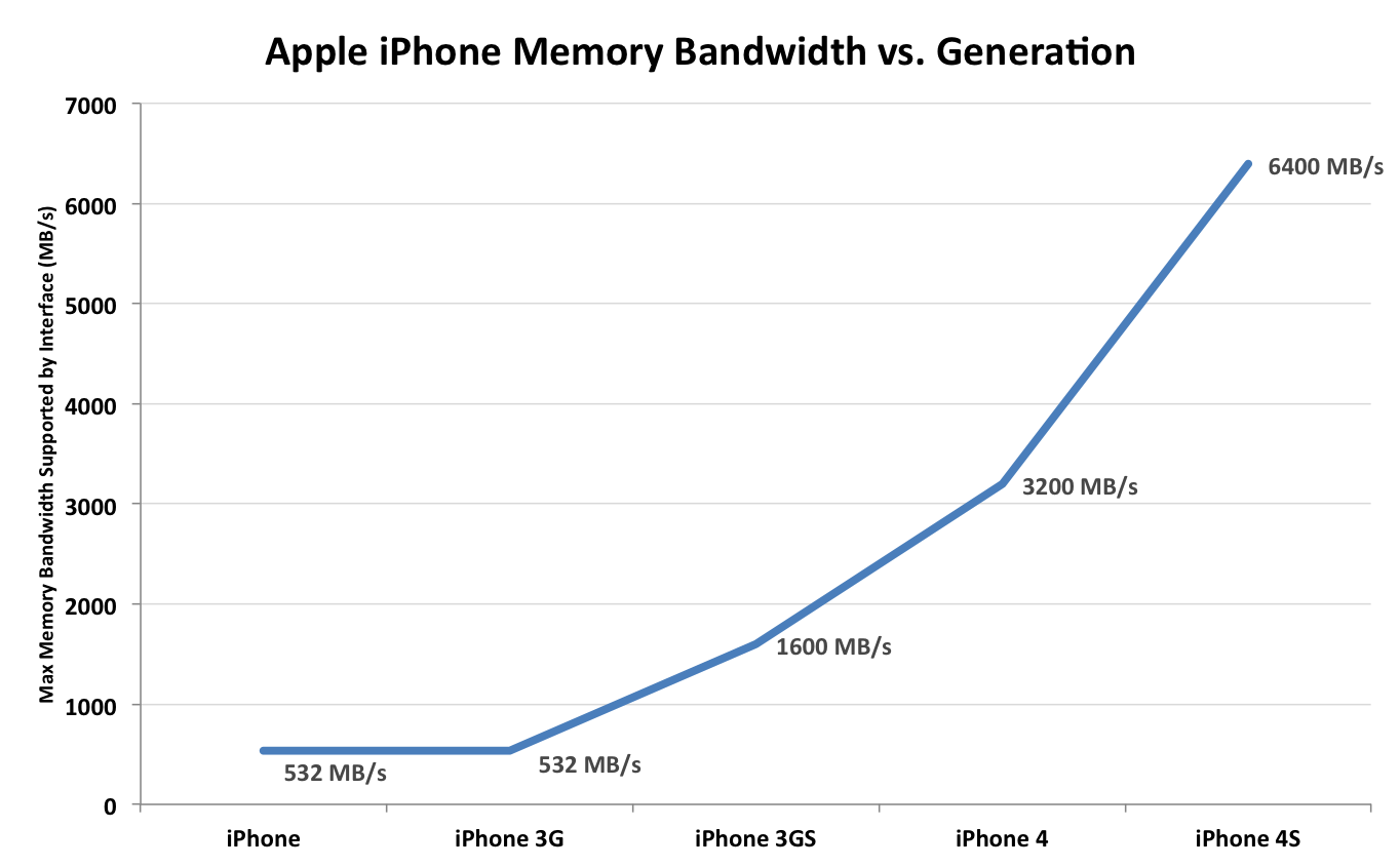
All of this tells us that the iPhone 4's A4 SoC has a 64-bit wide LPDDR1 memory interface with a 400MHz data rate. Multiply all of that out and you get peak theoretical bandwidth of 3.2GB/s. DDR memory interfaces are generally 80% efficient at best so you're looking at a limit of around 2.5GB/s. To put this in perspective, the A4 has as much memory bandwidth as the original AMD Athlon 64 released in 2003.
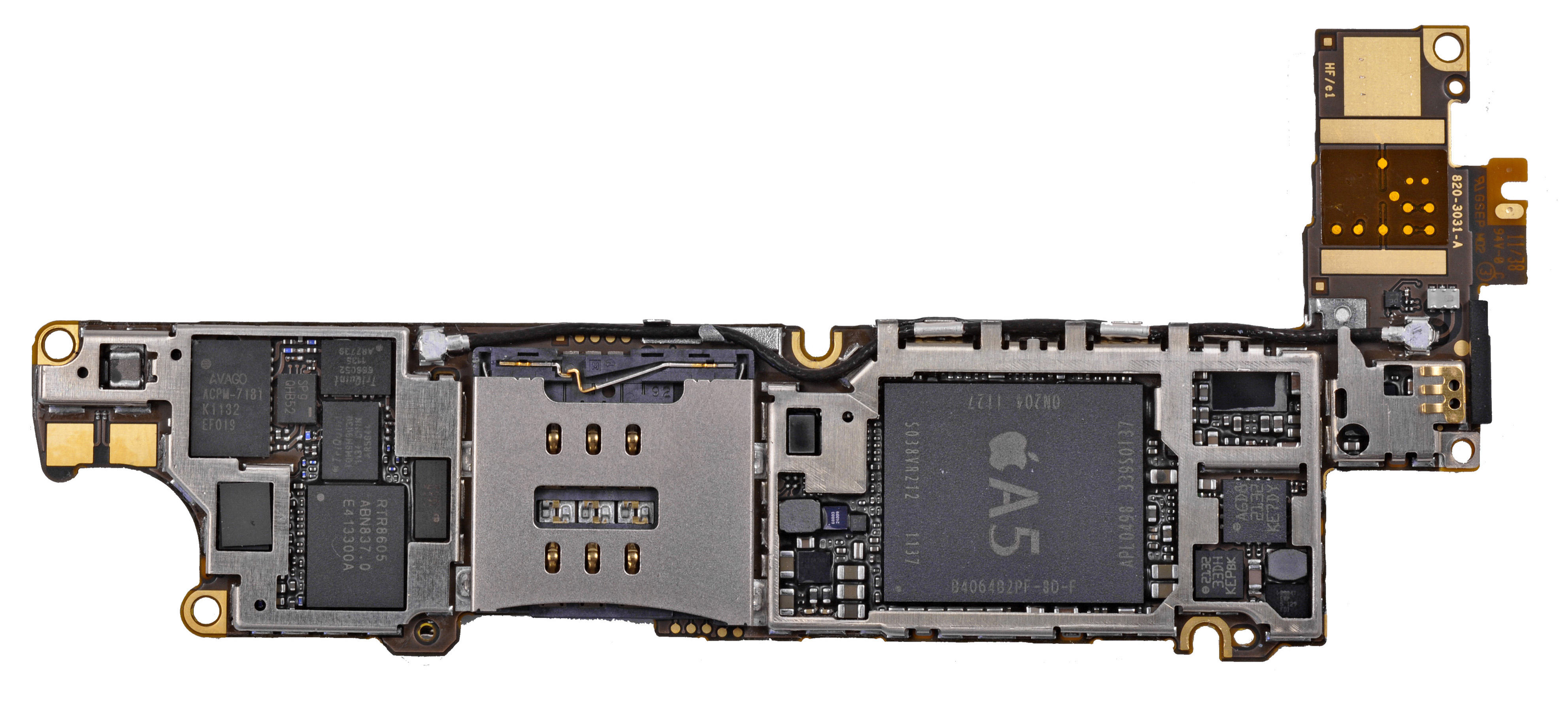
iPhone 4S mainboard, courtesy iFixit
With the A5 Apple definitely stepped up the memory interface. Once again we turn to iFixit's teardown of the iPhone 4S to lift that oh-so-precious part number: K3PE4E400B-XGC1.
The K once again tells us we're dealing with Samsung memory, while the 3P reveals there are two mobile DDR2 with 4n prefetch (aka LPDDR2-S4) DRAM die on the package. Why not a 4 this time? Technically the 4 refers to a discrete DRAM while the 3 implies a DRAM stack, obviously both are stacked DRAM so I'm not entirely sure why there's a difference here. Each of the next two E4s tell us the density of the two DRAM die. Samsung's public documentation only goes up to E3 which corresponds to a 1Gbit x32 device. Given that we know the A5 has 512MB on-package, E4 likely means 2Gbit x32 (256MB 32-bit). There are two E4 die on package which makes up the 512MB 64-bit DRAM stack.
Once again the final two characters reveal the cycle time of the DRAM: 2.5ns. The inverse of 2.5ns gives us a 400MHz clock frequency, or an 800MHz data rate (source clock frequency is actually 200MHz, but with a 4n prefetch we can transfer at effectively 800MHz). Peak bandwidth to the A5 is roughly double that of the A4: 6.4GB/s. This is as much memory bandwidth as AMD's Athlon 64 platform offered in late 2004, just 7 years later and in a much smaller form factor.
The doubling of memory bandwidth requires a sufficiently large workload to really show it. We see this in Geekbench's memory bandwidth results where the A5 doesn't appear to offer any more bandwidth than the A4 in all but one of the tests:
| Memory Bandwidth Comparison - Geekbench 2 | ||||
| Apple iPhone 4 | Apple iPhone 4S | |||
| Overall Memory Score | 593 | 700 | ||
| Read Sequential | 318.7 MB/s | 302.3 MB/s | ||
| Write Sequential | 704.9 MB/s | 809.2 MB/s | ||
| Stdlib Allocate | 1.55 Mallocs/sec | 1.55 Mallocs/sec | ||
| Stdlib Write | 1.25 GB/s | 2.54 GB/s | ||
| Stdlib Copy | 724.5 MB/s | 490.1 MB/s | ||
| Overall Stream Score | 280 | 281 | ||
| Stream Copy | 413.5 MB/s | 396.4 MB/s | ||
| Stream Scale | 313.3 MB/s | 317.4 MB/s | ||
| Stream Add | 518.0 MB/s | 527.1 MB/s | ||
| Stream Triad | 363.6 MB/s | 373.9 MB/s | ||
Memory bandwidth tests are extremely sensitive to architecture optimizations, particularly for single threaded tests like these so I wouldn't read too much into the cases where you see no gains or a drop.
The increase in raw memory bandwidth makes a lot of sense. Apple doubled the number of CPU cores on the A5, with each one even more bandwidth hungry than the single A4 core. The 4x increase in GPU compute combined with an increase in clock speeds give the A5 another big consumer of bandwidth. Add things like 1080p video capture and the memory bandwidth increase seems justified.
Looking back at the evolution of the iPhone's memory interface gives us an idea of just how quickly this industry has been evolving. Back in 2007 the original iPhone debuted with a 16-bit wide LPDDR-266 memory interface connected to a meager 128MB of DRAM. The 3GS delivered a huge increase in memory bandwidth by doubling the interface width and increasing the data rate to 400MHz. Scaling since then has been even more dramatic:
Memory capacity on the other hand has seen more of a step-function growth:
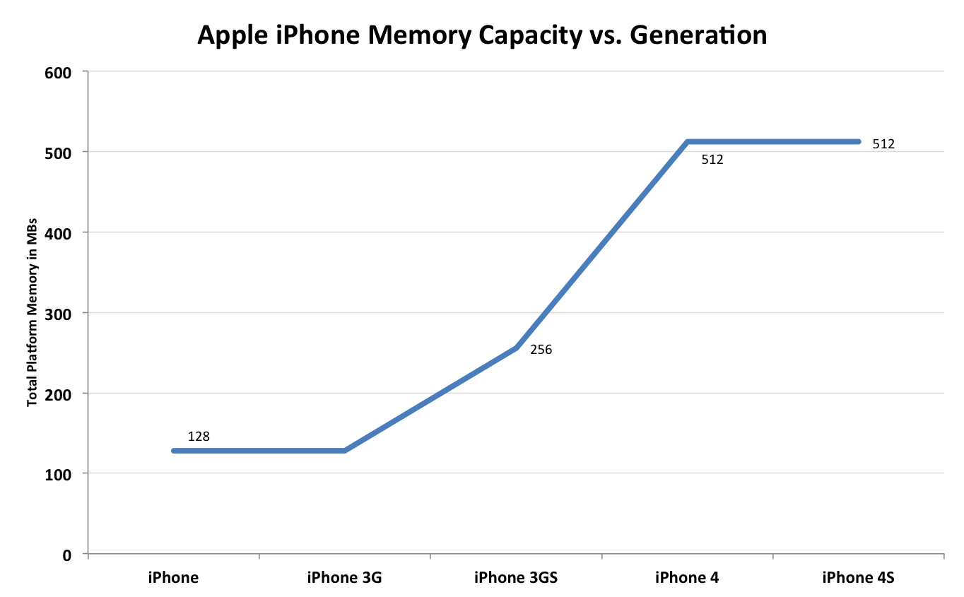
By using a mobile optimized OS Apple has been able to get around large memory requirements. The growth pattern in memory size partially illustrates the lag between introducing faster hardware and developers building truly demanding applications that require that sort of performance. Apple was able to leave the iPhone 4S at 512MB of RAM because the target for many iOS apps is still the iPhone 3GS generation. Don't be surprised to see a move to 1GB in the next iPhone release (we won't see 768MB due to the dual-channel memory requirement) as the app developer target moves to 512MB.


199 Comments
View All Comments
doobydoo - Friday, December 2, 2011 - link
Its still absolute nonsense to claim that the iPhone 4S can only use '2x' the power when it has available power of 7x.Not only does the iPhone 4s support wireless streaming to TV's, making performance very important, there are also games ALREADY out which require this kind of GPU in order to run fast on the superior resolution of the iPhone 4S.
Not only that, but you failed to take into account the typical life-cycle of iPhones - this phone has to be capable of performing well for around a year.
The bottom line is that Apple really got one over all Android manufacturers with the GPU in the iPhone 4S - it's the best there is, in any phone, full stop. Trying to turn that into a criticism is outrageous.
PeteH - Tuesday, November 1, 2011 - link
Actually it is about the architecture. How GPU performance scales with size is in large part dictated by the GPU architecture, and Imagination's architecture scales better than the other solutions.loganin - Tuesday, November 1, 2011 - link
And I showed it above Apple's chip isn't larger than Samsung's.PeteH - Tuesday, November 1, 2011 - link
But chip size isn't relevant, only GPU size is.All I'm pointing out is that not all GPU architectures scale equivalently with size.
loganin - Tuesday, November 1, 2011 - link
But you're comparing two different architectures here, not two carrying the same architecture so the scalability doesn't really matter. Also is Samsung's GPU significantly smaller than A5's?Now we've discussed back and forth about nothing, you can see the problem with Lucian's argument. It was simply an attempt to make Apple look bad and the technical correctness didn't really matter.
PeteH - Tuesday, November 1, 2011 - link
What I'm saying is that Lucian's assertion, that the A5's GPU is faster because it's bigger, ignores the fact that not all GPU architectures scale the same way with size. A GPU of the same size but with a different architecture would have worse performance because of this.Put simply architecture matters. You can't just throw silicon at a performance problem to fix it.
metafor - Tuesday, November 1, 2011 - link
Well, you can. But it might be more efficient not to. At least with GPU's, putting two in there will pretty much double your performance on GPU-limited tasks.This is true of desktops (SLI) as well as mobile.
Certain architectures are more area-efficient. But the point is, if all you care about is performance and can eat the die-area, you can just shove another GPU in there.
The same can't be said of CPU tasks, for example.
PeteH - Tuesday, November 1, 2011 - link
I should have been clearer. You can always throw area at the problem, but the architecture dictates how much area is needed to add the desired performance, even on GPUs.Compare the GeForce and the SGX architectures. The GeForce provides an equal number of vertex and pixel shader cores, and thus can only achieve theoretical maximum performance if it gets an even mix of vertex and pixel shader operations. The SGX on the other hand provides general purpose cores that work can do either vertex or pixel shader operations.
This means that as the SGX adds cores it's performance scales linearly under all scenarios, while the GeForce (which adds a vertex and a pixel shader core as a pair) gains only half the benefit under some conditions. Put simply, if a GeForce core is limited by the number of pixel shader cores available, the addition of a vertex shader core adds no benefit.
Throwing enough core pairs onto silicon will give you the performance you need, but not as efficiently as general purpose cores would. Of course a general purpose core architecture will be bigger, but that's a separate discussion.
metafor - Tuesday, November 1, 2011 - link
I think you need to check your math. If you double the number of cores in a Geforce, you'll still gain 2x the relative performance.Double is a multiplier, not an adder.
If a task was vertex-shader bound before, doubling the number of vertex-shaders (which comes with doubling the number of cores) will improve performance by 100%.
Of course, in the case of 543MP2, we're not just talking about doubling computational cores.
It's literally 2 GPU's (I don't think much is shared, maybe the various caches).
Think SLI but on silicon.
If you put 2 Geforce GPU's on a single die, the effect will be the same: double the performance for double the area.
Architecture dictates the perf/GPU. That doesn't mean you can't simply double it at any time to get double the performance.
PeteH - Tuesday, November 1, 2011 - link
But I'm not talking about relative performance, I'm talking about performance per unit area added. When bound by one operation adding a core that supports a different operation is wasted space.So yes, doubling space always doubles relative performance, but adding 20 square millimeters means different things to the performance of different architectures.