Qualcomm's New Snapdragon S4: MSM8960 & Krait Architecture Explored
by Brian Klug & Anand Lal Shimpi on October 7, 2011 12:35 PM EST- Posted in
- Smartphones
- Snapdragon
- Arm
- Qualcomm
- Krait
- MDP
- Mobile
- SoCs
The Adreno 225 GPU
Qualcomm has historically been pretty silent about its GPU architectures. You'll notice that specific details of Adreno GPU execution resources have been absent from most of our SoC comparisons. Starting with MSM8960 however, this is starting to change.
The MSM8960 uses a current generation Adreno GPU with a couple of changes. Qualcomm calls this GPU the Adreno 225, a follow-on to Adreno 220. Subsequent Krait designs will use Adreno 3xx GPUs based on a brand new architecture.
As we discussed in our Samsung Galaxy S 2 review, Qualcomm's Adreno architecture is a tile based immediate mode renderer with early-z rejection. By Qualcomm's own admission, Adreno is somewhere in the middle of the rendering spectrum between IMRs and Imagination Technologies' TBDR architectures. One key difference is Adreno's tiling isn't as fine grained as IMG's.
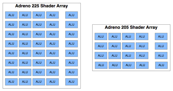
Architecturally the Adreno 225 and 220 are identical. Adreno 2xx is a DX9-class unified shader design. There's a ton of compute on-board with eight 4-wide vector units and eight scalar units. Each 4-wide vector unit is capable of a maximum of 8 MADs per clock, while each scalar unit is similarly capable of 2 MADs per clock. That works out to 160 floating point operations per clock, or 32 GFLOPS at 200MHz.
Update: Qualcomm has clarified the capabilities of its 4-wide Vector ALUs. Similar to the PowerVR SGX 543, each 4-wide vector ALU is capable of four MADs (one per component). The scalar units cannot be combined to do any MADs, although they are helpful we haven't really been tracking those in this table (IMG has something similar) so we've excluded them for now.
| Mobile SoC GPU Comparison | |||||||||||
| Adreno 225 | PowerVR SGX 540 | PowerVR SGX 543 | PowerVR SGX 543MP2 | Mali-400 MP4 | GeForce ULP | Kal-El GeForce | |||||
| SIMD Name | - | USSE | USSE2 | USSE2 | Core | Core | Core | ||||
| # of SIMDs | 8 | 4 | 4 | 8 | 4 + 1 | 8 | 12 | ||||
| MADs per SIMD | 4 | 2 | 4 | 4 | 4 / 2 | 1 | ? | ||||
| Total MADs | 32 | 8 | 16 | 32 | 18 | 8 | ? | ||||
| GFLOPS @ 200MHz | 12.8 GFLOPS | 3.2 GFLOPS | 6.4 GFLOPS | 12.8 GFLOPS | 7.2 GFLOPS | 3.2 GFLOPS | ? | ||||
| GFLOPS @ 300MHz | 19.2 GFLOPS | 4.8 GFLOPS | 9.6 GFLOPS | 19.2 GFLOPS | 10.8 GFLOPS | 4.8 GFLOPS | ? | ||||
Looking at the table above you'll see that this is the same amount of computing power than even IMG's PowerVR SGX 543MP2. However as we've already seen in our tests, Adreno 220 isn't anywhere near as quick.
Shader compiler efficiency and data requirements to actually populate a Vec4+1 array are both unknowns, and I suspect both significantly gate overall Adreno performance. There's also the fact that the Adreno 22x family only has two TMUs compared to four in the 543MP2, limiting texturing performance. Combine that with the fact that most Adreno 220 GPUs have been designed into single-channel memory controller systems and you've got a recipe for tons of compute potential limited by other bottlenecks.
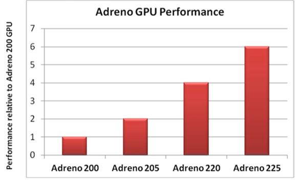
With Adreno 225 Qualcomm improves performance along two vectors, the first being clock speed. While Adreno 220 (used in the MSM8660) ran at 266MHz, Adreno 225 runs at 400MHz thanks to 28nm. Secondly, Qualcomm tells us Adreno 225 is accompanied by "significant driver improvements". Keeping in mind the sheer amount of compute potential of the Adreno 22x family, it only makes sense that driver improvements could unlock a lot of performance. Qualcomm expects the 225 to be 50% faster than the outgoing 220
Qualcomm claims that MSM8960 will be able to outperform Apple's A5 in GLBenchmark 2.x at qHD resolutions. We'll have to wait until we have shipping devices in hand to really put that claim to the test, but if true it's good news for Krait as the A5 continues to be the high end benchmark for mobile GPU performance.
While Adreno 225 is only Direct3D feature level 9_3 compliant, Qualcomm insisted that when the time is right it will have a D3D11 capable GPU using its own IP - putting to rest rumors of Qualcomm looking to license a third party GPU in order to be competitive in Windows 8 designs. Although Qualcomm committed to delivering D3D11 support, it didn't commit to a timeframe.


108 Comments
View All Comments
metafor - Friday, October 7, 2011 - link
I believe the comparison was simple: dual-Krait compared to 4xA9. I claimed Krait would be much closer to A15 level than A9 -- I was right.I claimed that 2xA15 (and 2xKrait) will be far better than 4xA9. I hold to that but some may disagree. I can understand that point.
I claimed that both Krait and A15 were set to target similar frequencies (~2.5GHz) according to release -- I was right.
I claimed that Krait will initially be ~1.4-1.7GHz on 28LP and is planned to reach 2.5GHz on HKM -- I was right.
On every point, you disagreed with me -- and stated "I know for a fact that such and such". Did Krait turn out to be "a modified A9" as you claimed? No.
Is its projected performance and clockspeeds far closer to A15-class than A9? Yes.
Also, how often do you think that quad-core on your desktop actually gets utilized? Are you under the impression that multithreading is some kind of magical pixie dust that you sprinkle on to an OS kernel and all of a sudden, your applications will run faster?
Hint: Android is fully multithread capable -- 3.0 even includes a great pthread library implementation. That doesn't mean individual applications can actually be threaded or that they even can be. This should be common knowledge by now: only certain workloads are highly parallelizable.
FunBunny2 - Saturday, October 8, 2011 - link
-- This should be common knowledge by now: only certain workloads are highly parallelizable.Too many folks have never heard of Amdahl or his law.
metafor - Friday, October 7, 2011 - link
On top of that -- as we've discussed previously -- there is a very small subset of computationally intensive, highly thread-scalable applications out there. Specifically: compression, video transcoding and image processing (which will likely be the biggest performance-demanding app for the CPU on tablets what with the Photoshop Touch series).So yes, on 4xA9, that could potentially scale to all 4 cores. But here's the thing: those are all very NEON/FPU intensive applications.
And guess what subsystem was substantially improved in A15 compared to A9?
Double the data path width, unified load-store, fully out-of-order VFP + NEON and lower integer execution latency on top of that (which, IIRC, is what most image processing algorithms use).
Even assuming A15 runs at the same clockspeed as an A9, it would still be 2-3x faster in typical arithmetic-intensive workloads.
partylikeits1999 - Saturday, October 8, 2011 - link
Anybody who thinks that application performance can be predicted by simply by CPU clock speeds alone, is a fool who has no business posting on sites like this. Let it go.baritz - Friday, October 7, 2011 - link
In the Power vs. Temperature plot on page two, have the axis labels been reversed accidentally?The way I read the graph as it is, 40nm transistors can handle more power without getting hot, while 28nm transistors get hot very quickly with only a small increase in power.
metafor - Friday, October 7, 2011 - link
It seems pretty clear. As temperature increases (right on the X axis), 40G transistors consume more power (up in the Y axis). The power increase vs temperature increase curve of 28LP doesn't grow as fast.This, of course, has more to do with it being an LP process. 40LP transistors would have a similar curve.
Haserath - Saturday, October 8, 2011 - link
Metafor is right about the curve having to do with the process. His explanation kinda makes it seem like a temp increase causes the power increase though. It's the power increase that causes the temp increase, and "G" transistors are designed to handle more power without wasted heat(temperature increase) compared to "LP" transistors. There's also a second reason why 28nm is hotter than 40nm.If you have a certain amount of heat energy being produced at a certain power level, the 40nm transistors will be a certain temperature.
Now take that same amount of heat energy being produced, and shrink the transistors to half their size. This increases their temperature within the same power envelope.
Of course they labeled a thermal limit on the power side, because the holder of whatever phone this chip goes into is going to feel the heat coming from the chip due to how much power it's using(how much heat energy is put out), not just due to the temperature of the transistors
metafor - Saturday, October 8, 2011 - link
It's actually both :)This is a problem in a lot of circuit design. Power dissipation (both due to scattering and increase in resistance of the charge channel) increases with temperature. But temperature also increases as more power is dissipated. It's a positive feedback loop that just gets hotter and hotter.
When simulating a circuit, this problem has to be taken into account but simulating the heat dissipation is difficult so one can never be sure that a circuit wouldn't overheat under its own operation.
It's an on-going research area in academics of how to simulate such a situation beforehand and avoid it.
Haserath - Sunday, October 9, 2011 - link
Well, that is true.Basically, it's increasing the power of the chip, which increases heat energy output, that increases the temperature. And with that increase in temperature, comes an increase in power.
Heat dissipation is the only way for the chip to keep itself from burning up. It's just impossible to really tell how much can be dissipated under even certain conditions due to heat exchange kinetically between atoms, and most likely the radiation amount differs between atoms.
It's basically impossible to simulate an exact scenario for this exchange.
jjj - Friday, October 7, 2011 - link
The minute a company gives you a bit of attention,you forget about objectivity."The key is this: other than TI's OMAP 5 in the second half of 2012 and Qualcomm's Krait, no one else has announced plans to release a new microarchitecture in the near term"
"Qualcomm remains the only active player in the smartphone/tablet space that uses its architecture license to put out custom designs."
Both statements are false,and you know that very well.