Qualcomm's New Snapdragon S4: MSM8960 & Krait Architecture Explored
by Brian Klug & Anand Lal Shimpi on October 7, 2011 12:35 PM EST- Posted in
- Smartphones
- Snapdragon
- Arm
- Qualcomm
- Krait
- MDP
- Mobile
- SoCs
Cache & Memory Hierarchy
Qualcomm has a three level exclusive cache hierarchy in Krait. The lower two levels are private per core, while the third level is shared among all cores. Qualcomm calls these caches L0, L1 and L2.
Each Krait core has an 8KB L0 cache (4KB instruction + 4KB data cache). The L0 cache is direct mapped and accessible in a single cycle. Qualcomm claims an 85% hit rate in this level 0 cache, which helps save power by not firing up the larger L1 cache. The hierarchy is exclusive so L0 data isn't necessarily duplicated in L1.
Each core also has a 32KB L1 cache (16KB instruction + 16KB data). The L1 4-way set associative and can also be accessed in a single cycle. There's no way prediction at work here. With 1 cycle latency to both L0 and L1, the primary advantage here is power.
| Krait Cache Architecture | |||||
| Size | Architecture | Frequency | |||
| L0 | 4KB + 4KB | Direct Mapped | Core | ||
| L1 | 16KB + 16KB | 4-way set associative | Core | ||
| L2 | 1MB (dual core) or 2MB (quad core) | 8-way set associative | 1.3GHz max | ||
The L2 cache is shared among all cores. In dual-core designs the L2 cache is sized at 1MB (up from 512KB in Scorpion), while quad-core Krait SoCs will have a 2MB L2. Krait's L2 cache is 8-way set associative.
While the L0 and L1 caches operate at core frequency and are on the same voltage plane as their associated core, the L2 cache is separate. To save power the L2 cache runs at its own frequency (up to 1.3GHz depending on the currently requested performance level). The L2 cache is on its own power plane and can be power gated if necessary.
Although Scorpion featured a dual-channel LPDDR2 memory controller, in a PoP configuration only one channel was available to any stacked DRAM. In order to get access to both 32-bit memory channels the OEM had to implement a DRAM on-package as well as an external DRAM on the PCB. Memory requests could be interleaved between the two DRAM, however Qualcomm seemed to prefer load balancing between the two with CPU/GPU accesses being directed to the lower latency PoP DRAM. Very few OEMs seemed to populate both channels and thus Scorpion based designs were effectively single-channel offerings.
Krait removes this limitation and now OEMs can utilize both memory channels in a PoP configuration (simply put two 32-bit DRAM die on the PoP stack) or in an external configuration. The split PoP/external DRAM organization is no longer supported. This change will hopefully mean we'll see more dual-channel Krait designs than we saw with Scorpion, which will in turn improve performance.
Process Technology and Clock Speeds
Krait will be the world's first smartphone CPU built on a 28nm process. Qualcomm is working with both TSMC and Global Foundries, although TSMC will produce the first chips. Krait will be built, at first, on TSMC's standard 28nm LP process. According to Qualcomm there's less risk associated with TSMC's non-HKMG process. Qualcomm was quick to point out that the entire MSM8960 SoC is built on a 28nm LP process compared to NVIDIA's 40nm LPG design in Kal-El. From Qualcomm's perspective, 40nm G transistors are only useful at reducing leakage at high temperatures but for the majority of the time a homogeneous LP design makes more sense.
Just like Scorpion, Krait places each core on its own voltage plane driven at its own clock frequency. Cores can be clocked independently of one another, which Qualcomm insists gives it a power advantage in many workloads.
The first implementation of Krait will be in a dual-core 1.5GHz MSM8960, however a second revision of the silicon will be introduced next year that increases clock speed to 1.7 - 2.0GHz. Qualcomm claims that at the same 1.05V core voltage, Krait can run at 1.7GHz vs. 1.55GHz for Scorpion. At these two clock speeds and at the same voltage, Qualcomm tells us that Krait consumes 265mW of power vs. 432mW running an undisclosed workload. Although it should be possible to draw more power than Scorpion under load, Krait should hopefully be able to improve overall power efficiency by completing tasks quicker and thus dropping down to idle faster than its predecessor. Smartphone and tablet battery life should remain the same at worst and improve at best, as a result.


108 Comments
View All Comments
metafor - Friday, October 7, 2011 - link
I believe the comparison was simple: dual-Krait compared to 4xA9. I claimed Krait would be much closer to A15 level than A9 -- I was right.I claimed that 2xA15 (and 2xKrait) will be far better than 4xA9. I hold to that but some may disagree. I can understand that point.
I claimed that both Krait and A15 were set to target similar frequencies (~2.5GHz) according to release -- I was right.
I claimed that Krait will initially be ~1.4-1.7GHz on 28LP and is planned to reach 2.5GHz on HKM -- I was right.
On every point, you disagreed with me -- and stated "I know for a fact that such and such". Did Krait turn out to be "a modified A9" as you claimed? No.
Is its projected performance and clockspeeds far closer to A15-class than A9? Yes.
Also, how often do you think that quad-core on your desktop actually gets utilized? Are you under the impression that multithreading is some kind of magical pixie dust that you sprinkle on to an OS kernel and all of a sudden, your applications will run faster?
Hint: Android is fully multithread capable -- 3.0 even includes a great pthread library implementation. That doesn't mean individual applications can actually be threaded or that they even can be. This should be common knowledge by now: only certain workloads are highly parallelizable.
FunBunny2 - Saturday, October 8, 2011 - link
-- This should be common knowledge by now: only certain workloads are highly parallelizable.Too many folks have never heard of Amdahl or his law.
metafor - Friday, October 7, 2011 - link
On top of that -- as we've discussed previously -- there is a very small subset of computationally intensive, highly thread-scalable applications out there. Specifically: compression, video transcoding and image processing (which will likely be the biggest performance-demanding app for the CPU on tablets what with the Photoshop Touch series).So yes, on 4xA9, that could potentially scale to all 4 cores. But here's the thing: those are all very NEON/FPU intensive applications.
And guess what subsystem was substantially improved in A15 compared to A9?
Double the data path width, unified load-store, fully out-of-order VFP + NEON and lower integer execution latency on top of that (which, IIRC, is what most image processing algorithms use).
Even assuming A15 runs at the same clockspeed as an A9, it would still be 2-3x faster in typical arithmetic-intensive workloads.
partylikeits1999 - Saturday, October 8, 2011 - link
Anybody who thinks that application performance can be predicted by simply by CPU clock speeds alone, is a fool who has no business posting on sites like this. Let it go.baritz - Friday, October 7, 2011 - link
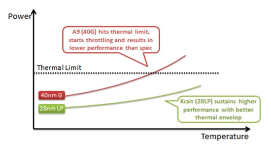
In the Power vs. Temperature plot on page two, have the axis labels been reversed accidentally?The way I read the graph as it is, 40nm transistors can handle more power without getting hot, while 28nm transistors get hot very quickly with only a small increase in power.
metafor - Friday, October 7, 2011 - link
It seems pretty clear. As temperature increases (right on the X axis), 40G transistors consume more power (up in the Y axis). The power increase vs temperature increase curve of 28LP doesn't grow as fast.This, of course, has more to do with it being an LP process. 40LP transistors would have a similar curve.
Haserath - Saturday, October 8, 2011 - link
Metafor is right about the curve having to do with the process. His explanation kinda makes it seem like a temp increase causes the power increase though. It's the power increase that causes the temp increase, and "G" transistors are designed to handle more power without wasted heat(temperature increase) compared to "LP" transistors. There's also a second reason why 28nm is hotter than 40nm.If you have a certain amount of heat energy being produced at a certain power level, the 40nm transistors will be a certain temperature.
Now take that same amount of heat energy being produced, and shrink the transistors to half their size. This increases their temperature within the same power envelope.
Of course they labeled a thermal limit on the power side, because the holder of whatever phone this chip goes into is going to feel the heat coming from the chip due to how much power it's using(how much heat energy is put out), not just due to the temperature of the transistors
metafor - Saturday, October 8, 2011 - link
It's actually both :)This is a problem in a lot of circuit design. Power dissipation (both due to scattering and increase in resistance of the charge channel) increases with temperature. But temperature also increases as more power is dissipated. It's a positive feedback loop that just gets hotter and hotter.
When simulating a circuit, this problem has to be taken into account but simulating the heat dissipation is difficult so one can never be sure that a circuit wouldn't overheat under its own operation.
It's an on-going research area in academics of how to simulate such a situation beforehand and avoid it.
Haserath - Sunday, October 9, 2011 - link
Well, that is true.Basically, it's increasing the power of the chip, which increases heat energy output, that increases the temperature. And with that increase in temperature, comes an increase in power.
Heat dissipation is the only way for the chip to keep itself from burning up. It's just impossible to really tell how much can be dissipated under even certain conditions due to heat exchange kinetically between atoms, and most likely the radiation amount differs between atoms.
It's basically impossible to simulate an exact scenario for this exchange.
jjj - Friday, October 7, 2011 - link
The minute a company gives you a bit of attention,you forget about objectivity."The key is this: other than TI's OMAP 5 in the second half of 2012 and Qualcomm's Krait, no one else has announced plans to release a new microarchitecture in the near term"
"Qualcomm remains the only active player in the smartphone/tablet space that uses its architecture license to put out custom designs."
Both statements are false,and you know that very well.