Qualcomm's New Snapdragon S4: MSM8960 & Krait Architecture Explored
by Brian Klug & Anand Lal Shimpi on October 7, 2011 12:35 PM EST- Posted in
- Smartphones
- Snapdragon
- Arm
- Qualcomm
- Krait
- MDP
- Mobile
- SoCs
Let's recap the current smartphone/tablet SoC landscape. Everything shipping today is built on a 4x-nm process, built either at Global Foundries, Samsung, TSMC or UMC. Next year we'll see a move to 28nm (bringing better performance and power characteristics) but between now and the end of 2012 there will be a myriad of designs available on the market.
The table below encapsulates much of what you can expect over the next 12+ months:
| 2011/2012 SoC Comparison | |||||||
| SoC | Process Node | CPU | GPU | Memory Bus | Release | ||
| Apple A5 | 45nm | 2 x ARM Cortex A9 w/ MPE @ 1GHz | PowerVR SGX 543MP2 | 2 x 32-bit LPDDR2 | Now | ||
| NVIDIA Tegra 2 | 40nm | 2 x ARM Cortex A9 @ 1GHz | GeForce | 1 x 32-bit LPDDR2 | Now | ||
| NVIDIA Tegra 3/Kal-El | 40nm | 4 x ARM Cortex A9 w/ MPE @ ~1.3GHz | GeForce++ | 1 x 32-bit LPDDR2 | Q4 2011 | ||
| Samsung Exynos 4210 | 45nm | 2 x ARM Cortex A9 w/ MPE @ 1.2GHz | ARM Mali-400 MP4 | 2 x 32-bit LPDDR2 | Now | ||
| Samsung Exynos 4212 | 32nm | 2 x ARM Cortex A9 w/ MPE @ 1.5GHz | ARM Mali-400 MP4 | 2 x 32-bit LPDDR2 | 2012 | ||
| ST-Ericsson NovaThor LP9600 (Nova A9600) | 28nm | 2 x ARM Cortex-A15 @ 2.5GHz | IMG PowerVR Series 6 (Rogue) | Dual Memory | 2013 | ||
| ST-Ericsson Novathor L9540 (Nova A9540) | 32nm | 2 x ARM Cortex A9 @ 1.85GHz | IMG PowerVR Series 5 | 2 x 32-bit LPDDR2 | 2H 2012 | ||
| ST-Ericsson NovaThor U9500 (Nova A9500) | 45nm | 2 x ARM Cortex A9 @ 1.2GHz | ARM Mali-400 MP1 | 1 x 32-bit LPDDR2 | Now | ||
| ST-Ericsson NovaThor U8500 | 45nm | 2 x ARM Cortex A9 @ 1.0GHz | ARM Mali-400 MP1 | 1 x 32-bit LPDDR2 | Now | ||
| TI OMAP 4430 | 45nm | 2 x ARM Cortex A9 w/ MPE @ 1.2GHz | PowerVR SGX 540 | 2 x 32-bit LPDDR2 | Now | ||
| TI OMAP 4460 | 45nm | 2 x ARM Cortex A9 w/ MPE @ 1.5GHz | PowerVR SGX 540 | 2 x 32-bit LPDDR2 | Q4 11 - 1H 12 | ||
| TI OMAP 4470 | 45nm | 2 x ARM Cortex A9 w/ MPE @ 1.8GHz | PowerVR SGX 544 | 2 x 32-bit LPDDR2 | 1H 2012 | ||
| TI OMAP 5 | 28nm | 2 x ARM Cortex A15 @ 2GHz | PowerVR SGX 544MPx | 2 x 32-bit LPDDR2 | 2H 2012 | ||
| Qualcomm MSM8x60 | 45nm | 2 x Scorpion @ 1.5GHz | Adreno 220 | 1 x 32-bit LPDDR2* | Now | ||
| Qualcomm MSM8960 | 28nm | 2 x Krait @ 1.5GHz | Adreno 225 | 2 x 32-bit LPDDR2 | 1H 2012 | ||
The key is this: other than TI's OMAP 5 in the second half of 2012 and Qualcomm's Krait, no one else has announced plans to release a new microarchitecture in the near term. Furthermore, if we only look at the first half of next year, Qualcomm is the only company that's focused on significantly improving per-core performance through a new architecture. Everyone else is either scaling up in core count (NVIDIA) or clock speeds. As we've seen in the PC industry however, generational performance gaps are hard to overcome - even with more cores or frequency.
Qualcomm has an ARM architecture license enabling it to build its own custom micro architectures that implement the ARM instruction set. This is similar to how AMD has an x86 license but designs its own chips rather than just producing clones of Intel processors. Qualcomm remains the only active player in the smartphone/tablet space that uses its architecture license to put out custom designs. The benefit to a custom design is typically better power and performance characteristics compared to the more easily synthesizable designs you get directly from ARM. The downside is development time and costs go up tremendously.
Scorpion was Qualcomm's first Snapdragon CPU architecture. At a high level, it looked very much like an optimized ARM Cortex A8 design although the two had nothing in common outside of instruction set. Scorpion was a dual-issue, in-order architecture that eventually scaled to dual-core and 1.5GHz variants.
Scorpion was pretty much the CPU architecture of choice in the 2009 - 2010 timeframe. Throughout 2011 however, Qualcomm has been very quiet as dual Cortex A9 designs from NVIDIA, Samsung and TI have surpassed it in terms of performance.
Going into 2012, Qualcomm is set for a return to glory as it will be the first to deliver a brand new microprocessor architecture and the first to ship 28nm SoCs in volume. Qualcomm's next-generation SoCs will also be the first to integrate an LTE modem on-die, which should enable LTE on nearly all high-end devices at much better power levels than current multi-chip 4x-nm solutions. Today we're able to talk a bit about the architecture details and performance expectations of Qualcomm's next-generation SoC due out in the first half of 2012.
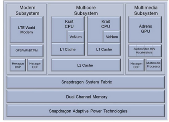
Krait Architecture

The Krait processor is the heart of Qualcomm's second generation Snapdragon and it's the core of all Snapdragon S4 SoCs. Krait takes the aging base of Scorpion and gives it a much needed dose of adrenaline.
Krait's front end is significantly wider. The architecture can fetch and decode three instructions per clock. The decoders are equally capable of decoding any ARMv7-A instructions. The wider front end is a significant improvement over the 2-wide Scorpion core. It alone will be responsible for a tangible increase in IPC.
| Architecture Comparison | ||||||||
| ARM11 | ARM Cortex A8 | ARM Cortex A9 | Qualcomm Scorpion | Qualcomm Krait | ||||
| Decode | single-issue | 2-wide | 2-wide | 2-wide | 3-wide | |||
| Pipeline Depth | 8 stages | 13 stages | 8 stages | 10 stages | 11 stages | |||
| Out of Order Execution | N | N | Y | Partial | Y | |||
| FPU | VFP11 (pipelined) | VFPv3 (not-pipelined) | Optional VFPv3-D16 (pipelined) | VFPv3 (pipelined) | VFPv3 (pipelined) | |||
| NEON | N/A | Y (64-bit wide) | Optional MPE (64-bit wide) | Y (128-bit wide) | Y (128-bit wide) | |||
| Process Technology | 90nm | 65nm/45nm | 40nm | 40nm | 28nm | |||
| Typical Clock Speeds | 412MHz | 600MHz/1GHz | 1.2GHz | 1GHz | 1.5GHz | |||
The execution back-end receives a similar expansion. Whereas the original Scorpion core only had three ports to its execution units, Krait increases that to seven. Krait can issue up to four instructions in parallel. The additional execution ports simply help prevent any artificial constraints on ILP. This is another area where Krait will be able to see significant IPC gains.
Krait's fetch and decode stages are obviously in-order, but the back-end is entirely out-of-order. Qualcomm claims that any instruction can be executed out of order, assuming that doing so doesn't create any new hazards. Instructions are retired in order.
Qualcomm lengthened Krait's integer pipeline slightly from 10 stages in Scorpion to 11 stages in Krait. Load/store operations tack on another two cycles and instructions that go through the Neon/VFP path further lengthen the pipe. ARM's Cortex A15 design by comparison features a 15-stage integer pipeline. Qualcomm's design does contain more custom logic than ARM's stock A15, which has typically given it a clock speed advantage. The A15's deeper pipeline should give it a clock speed advantage as well. Whether the two effectively cancel each other out remains to be seen.
| Qualcomm Architecture Comparison | ||||
| Scorpion | Krait | |||
| Pipeline Depth | 10 stages | 11 stages | ||
| Decode | 2-wide | 3-wide | ||
| Issue Width | 3-wide? | 4-wide | ||
| Execution Ports | 3 | 7 | ||
| L2 Cache (dual-core) | 512KB | 1MB | ||
| Core Configurations | 1, 2 | 1, 2, 4 | ||
Krait has been upgraded to support the new virtualization instructions added in Cortex A15. Also like the A15, Krait enables LPAE for 40-bit memory addressing.
At a high-level Qualcomm has built a 3-wide, out-of-order engine that feels very much like a modern version of Intel's old P6. Whereas designs from the A8 generation looked like modern Pentiums, Krait takes us into the era of the Pentium II.
Note that courtesy of the wider front-end and OoO execution engine, Krait should be a higher performance architecture than Intel's Atom. That's right, you'll be able to get better performance than some of the very first Centrino notebooks in your smartphones come 2012.
Performance Expectations
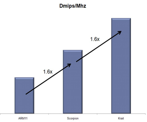
Performance of ARM cores has always been characterized by DMIPS (Dhrystone Millions of Instructions per Second). An extremely old integer benchmark, Dhrystone was popular in the PC market when I was growing up but was abandoned long ago in favor of more representative benchmarks. You can get a general idea of performance improvements across similar architectures assuming there are no funny compiler tricks at play. The comparison of single-core DMIPS/MHz is below:
| ARM DMIPS/MHz | ||||||||
| ARM11 | ARM Cortex A8 | ARM Cortex A9 | Qualcomm Scorpion | Qualcomm Krait | ||||
| DMIPS/MHz | 1.25 | 2.0 | 2.5 | 2.1 | 3.3 | |||
At 3.3, Krait should be around 30% faster than a Cortex A9 running at the same frequency. At launch Krait will run 25% faster than most A9s on the market today, a gap that will only grow as Qualcomm introduces subsequent versions of the core. It's not unreasonable to expect a 30 - 50% gain in performance over existing smartphone designs. ARM hasn't published DMIPS/MHz numbers for the Cortex A15, although rumors place its performance around 3.5 DMIPS/MHz.
Updated VeNum Unit
ARM's NEON instruction set is handled by a dedicated unit in all of its designs. Krait is no different. Qualcomm calls its NEON engine VeNum and has increased its issue capabilities by 50%. Whereas Scorpion could only issue two NEON instructions in parallel, Krait can do three.
Qualcomm's NEON data paths are still 128-bits wide.
Update: Qualcomm published its whitepaper on the Snapdragon S4. Check it out here.


108 Comments
View All Comments
metafor - Friday, October 7, 2011 - link
I believe the comparison was simple: dual-Krait compared to 4xA9. I claimed Krait would be much closer to A15 level than A9 -- I was right.I claimed that 2xA15 (and 2xKrait) will be far better than 4xA9. I hold to that but some may disagree. I can understand that point.
I claimed that both Krait and A15 were set to target similar frequencies (~2.5GHz) according to release -- I was right.
I claimed that Krait will initially be ~1.4-1.7GHz on 28LP and is planned to reach 2.5GHz on HKM -- I was right.
On every point, you disagreed with me -- and stated "I know for a fact that such and such". Did Krait turn out to be "a modified A9" as you claimed? No.
Is its projected performance and clockspeeds far closer to A15-class than A9? Yes.
Also, how often do you think that quad-core on your desktop actually gets utilized? Are you under the impression that multithreading is some kind of magical pixie dust that you sprinkle on to an OS kernel and all of a sudden, your applications will run faster?
Hint: Android is fully multithread capable -- 3.0 even includes a great pthread library implementation. That doesn't mean individual applications can actually be threaded or that they even can be. This should be common knowledge by now: only certain workloads are highly parallelizable.
FunBunny2 - Saturday, October 8, 2011 - link
-- This should be common knowledge by now: only certain workloads are highly parallelizable.Too many folks have never heard of Amdahl or his law.
metafor - Friday, October 7, 2011 - link
On top of that -- as we've discussed previously -- there is a very small subset of computationally intensive, highly thread-scalable applications out there. Specifically: compression, video transcoding and image processing (which will likely be the biggest performance-demanding app for the CPU on tablets what with the Photoshop Touch series).So yes, on 4xA9, that could potentially scale to all 4 cores. But here's the thing: those are all very NEON/FPU intensive applications.
And guess what subsystem was substantially improved in A15 compared to A9?
Double the data path width, unified load-store, fully out-of-order VFP + NEON and lower integer execution latency on top of that (which, IIRC, is what most image processing algorithms use).
Even assuming A15 runs at the same clockspeed as an A9, it would still be 2-3x faster in typical arithmetic-intensive workloads.
partylikeits1999 - Saturday, October 8, 2011 - link
Anybody who thinks that application performance can be predicted by simply by CPU clock speeds alone, is a fool who has no business posting on sites like this. Let it go.baritz - Friday, October 7, 2011 - link
In the Power vs. Temperature plot on page two, have the axis labels been reversed accidentally?The way I read the graph as it is, 40nm transistors can handle more power without getting hot, while 28nm transistors get hot very quickly with only a small increase in power.
metafor - Friday, October 7, 2011 - link
It seems pretty clear. As temperature increases (right on the X axis), 40G transistors consume more power (up in the Y axis). The power increase vs temperature increase curve of 28LP doesn't grow as fast.This, of course, has more to do with it being an LP process. 40LP transistors would have a similar curve.
Haserath - Saturday, October 8, 2011 - link
Metafor is right about the curve having to do with the process. His explanation kinda makes it seem like a temp increase causes the power increase though. It's the power increase that causes the temp increase, and "G" transistors are designed to handle more power without wasted heat(temperature increase) compared to "LP" transistors. There's also a second reason why 28nm is hotter than 40nm.If you have a certain amount of heat energy being produced at a certain power level, the 40nm transistors will be a certain temperature.
Now take that same amount of heat energy being produced, and shrink the transistors to half their size. This increases their temperature within the same power envelope.
Of course they labeled a thermal limit on the power side, because the holder of whatever phone this chip goes into is going to feel the heat coming from the chip due to how much power it's using(how much heat energy is put out), not just due to the temperature of the transistors
metafor - Saturday, October 8, 2011 - link
It's actually both :)This is a problem in a lot of circuit design. Power dissipation (both due to scattering and increase in resistance of the charge channel) increases with temperature. But temperature also increases as more power is dissipated. It's a positive feedback loop that just gets hotter and hotter.
When simulating a circuit, this problem has to be taken into account but simulating the heat dissipation is difficult so one can never be sure that a circuit wouldn't overheat under its own operation.
It's an on-going research area in academics of how to simulate such a situation beforehand and avoid it.
Haserath - Sunday, October 9, 2011 - link
Well, that is true.Basically, it's increasing the power of the chip, which increases heat energy output, that increases the temperature. And with that increase in temperature, comes an increase in power.
Heat dissipation is the only way for the chip to keep itself from burning up. It's just impossible to really tell how much can be dissipated under even certain conditions due to heat exchange kinetically between atoms, and most likely the radiation amount differs between atoms.
It's basically impossible to simulate an exact scenario for this exchange.
jjj - Friday, October 7, 2011 - link
The minute a company gives you a bit of attention,you forget about objectivity."The key is this: other than TI's OMAP 5 in the second half of 2012 and Qualcomm's Krait, no one else has announced plans to release a new microarchitecture in the near term"
"Qualcomm remains the only active player in the smartphone/tablet space that uses its architecture license to put out custom designs."
Both statements are false,and you know that very well.