AMD's Graphics Core Next Preview: AMD's New GPU, Architected For Compute
by Ryan Smith on December 21, 2011 9:38 PM ESTNot Just A New Architecture, But New Features Too
So far we’ve talked about Graphics Core Next as a new architecture, how that new architecture works, and what that new architecture does that Cayman and other VLIW architectures could not. But along with the new architecture GCN will bring with it a number of new compute features to further flesh out AMD’s GPU computing capabilities and to cement the GPU’s position as the CPU’s partner rather than a subservient peripheral.
In terms of base features the biggest change will be that GCN will implement the underlying features necessary to support C++ and other advanced languages. As a result GCN will be adding support for pointers, virtual functions, exception support, and even recursion. These underlying features mean that developers will not need to “step down” from higher languages to C to write code for the GPU, allowing them to more easily program for the GPU and CPU within the same application. For end-users the benefit won’t be immediate, but eventually it will allow for more complex and useful programs to be GPU accelerated.
Because the underlying feature set is evolving, the memory subsystem is also evolving to be able to service those features. The chief change here is that the hardware is being adapted to support an ISA that uses unified memory. This goes hand-in-hand with the earlier language features to allow programmers to write code to target both the CPU and the GPU, as programs (or rather compilers) can reference memory anywhere, without the need to explicitly copy memory from one device to the other before working on it. Now there’s still a significant performance impact when accessing off-GPU memory – particularly in the case of dGPUs where on-board memory is many times faster than system memory – so developers and compilers will still be copying data around to keep it close to the processor that’s going to use it, but this essentially becomes abstracted from developers.
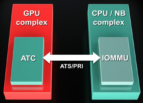
Now what’s interesting is that the unified address space that will be used is the x86-64 address space. All instructions sent to a GCN GPU will be relative to the x86-64 address space, at which point the GPU will be responsible for doing address translation to local memory addresses. In fact GCN will even be incorporating an I/O Memory Mapping Unit (IOMMU) to provide this functionality; previously we’ve only seen IOMMUs used for sharing peripherals in a virtual machine environment. GCN will even be able to page fault half-way gracefully by properly stalling until the memory fetch completes. How this will work with the OS remains to be seen though, as the OS needs to be able to address the IOMMU. GCN may not be fully exploitable under Windows 7.
Finally on the memory side, AMD is adding proper ECC support to supplement their existing EDC (Error Detection & Correction) functionality, which is used to ensure the integrity of memory transmissions across the GDDR5 memory bus. Both the SRAM and VRAM memory can be ECC protected. For the SRAM this is a free operation, while for the VRAM there will be a performance overhead. We’re assuming that AMD will be using a virtual ECC scheme like NVIDIA, where ECC data is distributed across VRAM rather than using extra memory chips/controllers.
Elsewhere we’ve already mentioned FP64 support. All GCN GPUs will support FP64 in some form, making FP64 support a standard feature across the entire lineup. The actual FP64 performance is configurable – the architecture supports ½ rate FP64, but ¼ rate and 1/16 rate are also options. We expect AMD to take a page from NVIDIA here and configure lower-end consumer parts to use the slower rates since FP64 is not currently important for consumer uses.
Finally, for programmers some additional hardware changes have been made to improve debug support by allowing debugging tools to tap the GPU at additional points. The new ISA for GCN will already make debugging easier, but this will further that goal. As with other developer features this won’t directly impact end-users, but it will ultimately lead to better software sooner as the features and tools available for debugging GPU programs have been well behind the well-established tools used for debugging CPU programs.


83 Comments
View All Comments
DoctorPizza - Monday, June 20, 2011 - link
I can't understand that at all.The next architecture will have 16-wide SIMD. How does that fit computational problems better than a 16-wide MIMD VLIW architecture? VLIW can act as if it were SIMD if necessary (simply make each instruction within the word the same, varying only the operands), so how on earth can SIMD be better? SIMD is strictly less general and less flexible than VLIW. This makes it applicable to a narrower set of problems--if you have problems that aren't 16-wide, then you're wasting those additional ALUs, and there's nothing you can do with them, ever. MIMD can't always use them, but there the restriction is unbreakable dependencies, not an inability to encode instructions.
And while VLIW heritage is indeed statically scheduled, nothing about VLIW mandates static scheduling. The next generation Itanium will use dynamic scheduling, for example.
This whole article reads like AMD has offered a rationale for its architectural change, and the author has accepted that rationale without ever stopping to consider if it makes sense.
DoctorPizza - Monday, June 20, 2011 - link
(FYI: the *real* reason to go for SIMD instead of VLIW is simply that VLIW takes up more die area. AMD has decided that the problems people are working on have enough data- and thread-level parallelism that it's not worth having extra decode logic to enable extraction of more instruction-level parallelism.The result is a design that's actually *worse* for general-purpose computation--for non-vector computations, it'll only ever use one of those sixteen ALUs, whereas the previous design could in principle use them all--but better for embarrassingly parallel workloads.
Why the article couldn't say this is anybody's guess.)
Quantumboredom - Tuesday, June 21, 2011 - link
I don't understand your argument. They have moved from 16-wide SIMD where each instruction is a 4-operation VLIW (where there are quite a few restrictions on what that VLIW instruction can actually be) to _four_ 16-wide SIMDs where each instruction is scalar. The new architecture is in every way more general and more suited to a wide range of computational problems while retaining the same power. It does presumably cost more (in terms of area/transistors), but hopefully it will be worth it.DoctorPizza - Tuesday, June 21, 2011 - link
Where does it say that Cayman SPs are ganged into groups of 16? It says they're grouped somehow, but never makes the claim that their groups are as wide as the new SIMD short vectors.Quantumboredom - Tuesday, June 21, 2011 - link
It is well-known that Cypress and Cayman both have arrays of 16 processing elements operating in SIMD mode, and they have to execute work-items from the same work-group over four cycles, leading to a wavefront size of 64. See for example the AMD APP OpenCL Programming Guide 1.3c section 1.2 where this is described. Specifically it says "All stream cores within a compute unit execute the same instruction sequence in lock-step".DoctorPizza - Tuesday, June 21, 2011 - link
"well-known"? I assure you, the vast majority of people have not read AMD's OpenCL Programming Guide.Nonetheless, the article still makes little sense.
A vector of 16 instruction-parallel processors is more versatile than a vector of 16 strictly SISD ones. In the worst case, with unbreakable data dependencies, the former degrades to the latter. In the best case, the former can do 4 (VLIW4) or 5 (VLIW5) times the work of the latter. The average case cited in the article was about 3.5 times.
If you only had one thread of work, the old architecture would tend to be better. For every 64 ALUs (one old VLIW vector or four new SIMD vectors), a single-threaded task would average usage of 56 out of 64 ALUs (3.5 per VLIW) on the old arch, but only 16 out of 64 on the new.
However, AMD is plainly counting on there being many, many potential threads. If you have abundant threads then you can guarantee that you can fill up the remaining 48 ALUs with different threads, whereas the 8 unused ALUs in the VLIW arch are off-limits.
This is a less general architecture, but as long as all your problems are massively parallel, creating all those extra threads shouldn't be a problem. AMD is sacrificing generality in favour of the embarrassingly parallel.
Quantumboredom - Tuesday, June 21, 2011 - link
I actually asked a similar question at the AMD Fusion Developer Summit.The minimum number of wavefronts (i.e., batches of 64 work-items) needed to keep a Cypress/Cayman CU fed is two, while GCN requires four wavefronts (so twice as many). However it is the case that quite often (for all of my programs actually) you really do need four wavefronts per CU on Cypress/Cayman to effectively hide the global memory latency. The guy I was talking to at AMD seemed to thnik that in practice the number of work-items needed would stay about the same between Cayman and GCN for most applications.
I've asked this question on the AMD developer forums as well, but I don't know how many answers will be given about GCN there.
DoctorPizza - Tuesday, June 21, 2011 - link
I certainly wouldn't be surprised to hear that typical GPGPU workloads could inundate the GPU with threads and so provide more than enough wavefronts. The GPGPU workloads are pretty much all of the embarrassingly parallel kind, so creating more threads should tend to be pretty trivial.So your experience certainly makes sense with what I'd expect.
It's not that I think this is necessarily a bad change for the applications that people use GPGPU processing for.
It's more that I'm disputing the implication that this somehow makes the GPU more general and easier to take advantage of; to my mind it's doing the exact opposite of that.
Or to put it another way: virtually every single program has a reasonable amount of instruction level parallelism. Data-/thread-level parallelism is much rarer. We're losing the former to improve the latter.
For problems amenable to massive thread-/data-level parallelism the result should be substantially more ALUs available to process on. But for problems with only limited data-/thread-level parallelism, it's a step backwards.
name99 - Thursday, December 22, 2011 - link
"The next architecture will have 16-wide SIMD. How does that fit computational problems better than a 16-wide MIMD VLIW architecture? VLIW can act as if it were SIMD if necessary (simply make each instruction within the word the same, varying only the operands), so how on earth can SIMD be better? SIMD is strictly less general and less flexible than VLIW."A VLIW system has to have instruction decoders and routers for every instruction, and thus for every data item that is processed.
A SIMD system only has to have one instruction decoder and router for every 16 data items that are processed. If your computations consist primarily of doing the same thing to multiple data items this is a win. (More processing for less power and less silicon.) If your computations do NOT consist primarily of doing the same thing to multiple data items, it's a loss.
Or, to put it differently, is it worth investing silicon in moving instructions around with great facility, or is it better to invest silicon in moving data around with great facility? Seymour Crane thought (for the problems he cared about) the answer was data. I'd like to think AMD know enough about what they are doing that they have the numbers in hand, and have calculated that, once again for them the answer is data.
MySchizoBuddy - Tuesday, June 21, 2011 - link
where is the information about the toolkit to take advantage of this hardware?