AMD's Graphics Core Next Preview: AMD's New GPU, Architected For Compute
by Ryan Smith on December 21, 2011 9:38 PM ESTAnd Many Compute Units Make A GPU
While the compute unit is the fundamental unit of computation, it is not a GPU on its own. As with SIMDs in Cayman it’s a configurable building block for making a larger GPU, with a GPU implementing a suitable number of CUs in multiples of 4. Like past GPUs this will be the primary way to scale the GPU to the desired die size, but of course this isn’t the only element of the design that scales.
With a suitable number of CUs in hand, it’s time to attach the rest of units that make up a GPU. As this is a high-level overview on the part of AMD they haven’t gone into great deal on what each unit does and how it does it, but as the first GCN product gets closer to launching the picture will take on a more complete form.
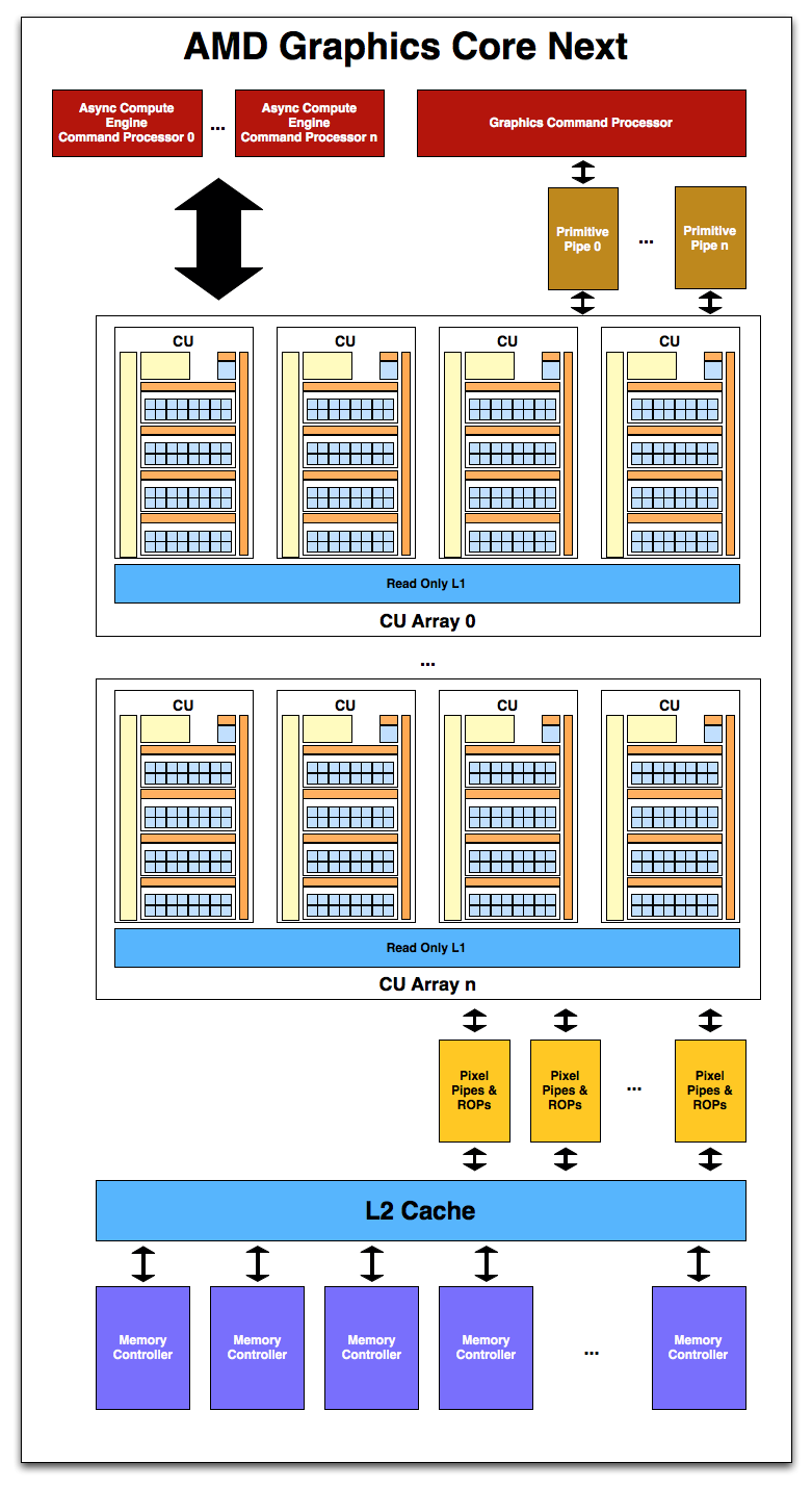
Starting with memory and cache, GCN will once more pair its L2 cache with its memory controllers. The architecture supports 64KB or 128KB of L2 cache per memory controller, and given that AMD’s memory controllers are typically 64bits each, this means a Cayman-like design would likely have 512KB of L2 cache. The L2 cache is write-back, and will be fully coherent so that all CUs will see the same data, saving expensive trips to VRAM for synchronization. CPU/GPU synchronization will also be handled at the L2 cache level, where it will be important to maintain coherency between the two in order to efficiently split up a task between the CPU and GPU. For APUs there is a dedicated high-speed bus between the two, while discrete GPUs will rely on PCIe’s coherency protocols to keep the CPU and dGPU in sync.
Meanwhile on the compute side, AMD’s new Asynchronous Compute Engines serve as the command processors for compute operations on GCN. The principal purpose of ACEs will be to accept work and to dispatch it off to the CUs for processing. As GCN is designed to concurrently work on several tasks, there can be multiple ACEs on a GPU, with the ACEs deciding on resource allocation, context switching, and task priority. AMD has not established an immediate relationship between ACEs and the number of tasks that can be worked on concurrently, so we’re not sure whether there’s a fixed 1:X relationship or whether it’s simply more efficient for the purposes of working on many tasks in parallel to have more ACEs.
One effect of having the ACEs is that GCN has a limited ability to execute tasks out of order. As we mentioned previously GCN is an in-order architecture, and the instruction stream on a wavefront cannot be reodered. However the ACEs can prioritize and reprioritize tasks, allowing tasks to be completed in a different order than they’re received. This allows GCN to free up the resources those tasks were using as early as possible rather than having the task consuming resources for an extended period of time in a nearly-finished state. This is not significantly different from how modern in-order CPUs (Atom, ARM A8, etc) handle multi-tasking.
On the other side of the coin we have the graphics hardware. As with Cayman a graphics command processor sits at the top of the stack and is responsible for farming out work to the various components of the graphics subsystem. Below that Cayman’s dual graphics engines have been replaced with multiple primitive pipelines, which will serve the same general purpose of geometry and fixed-function processing. Primative pipelines will be responsible for tessellation, geometry, and high-order surface processing among other things. Whereas Cayman was limited to 2 such units, GCN will be fully scalable, so AMD will be able to handle incredibly large amounts of geometry if necessary.
After a trip through the CUs, graphics work then hits the pixel pipelines, which are home to the ROPs. As it’s customary to have a number of ROPs, there will be a scalable number of pixel pipelines in GCN; we expect this will be closely coupled with the number of memory controllers to maintain the tight ROP/L2/Memory integration that’s so critical for high ROP performance.
Unfortunately, those of you expecting any additional graphics information will have to sit tight for the time being. As was the case with NVIDIA’s early reveal of Fermi in 2009, AFDS is a development show, and GCN’s early reveal is about the compute capabilities rather than the graphics capabilities. AMD needs to prime developers for GCN now, so that when GCN appears in an APU developers are ready for it. We’ll find out more about the capabilities of the ROPs, the primitive pipelines, the texture mapping units, the display controllers and other dedicated hardware blocks farther down the line.
In the meantime AMD did throw out one graphics tidbit: partially resident textures (PRT). PRTs allow for only part of a texture to actually be loaded in memory, allowing developers to use large textures without taking the performance hit of loading the entire texture into memory if parts of it are going unused. John Carmack already does something very similar in software with his MegaTexture technology, which is used in the id Tech 4 and id Tech 5 engines. This is essentially a hardware implementation of that technology.


83 Comments
View All Comments
DoctorPizza - Monday, June 20, 2011 - link
I can't understand that at all.The next architecture will have 16-wide SIMD. How does that fit computational problems better than a 16-wide MIMD VLIW architecture? VLIW can act as if it were SIMD if necessary (simply make each instruction within the word the same, varying only the operands), so how on earth can SIMD be better? SIMD is strictly less general and less flexible than VLIW. This makes it applicable to a narrower set of problems--if you have problems that aren't 16-wide, then you're wasting those additional ALUs, and there's nothing you can do with them, ever. MIMD can't always use them, but there the restriction is unbreakable dependencies, not an inability to encode instructions.
And while VLIW heritage is indeed statically scheduled, nothing about VLIW mandates static scheduling. The next generation Itanium will use dynamic scheduling, for example.
This whole article reads like AMD has offered a rationale for its architectural change, and the author has accepted that rationale without ever stopping to consider if it makes sense.
DoctorPizza - Monday, June 20, 2011 - link
(FYI: the *real* reason to go for SIMD instead of VLIW is simply that VLIW takes up more die area. AMD has decided that the problems people are working on have enough data- and thread-level parallelism that it's not worth having extra decode logic to enable extraction of more instruction-level parallelism.The result is a design that's actually *worse* for general-purpose computation--for non-vector computations, it'll only ever use one of those sixteen ALUs, whereas the previous design could in principle use them all--but better for embarrassingly parallel workloads.
Why the article couldn't say this is anybody's guess.)
Quantumboredom - Tuesday, June 21, 2011 - link
I don't understand your argument. They have moved from 16-wide SIMD where each instruction is a 4-operation VLIW (where there are quite a few restrictions on what that VLIW instruction can actually be) to _four_ 16-wide SIMDs where each instruction is scalar. The new architecture is in every way more general and more suited to a wide range of computational problems while retaining the same power. It does presumably cost more (in terms of area/transistors), but hopefully it will be worth it.DoctorPizza - Tuesday, June 21, 2011 - link
Where does it say that Cayman SPs are ganged into groups of 16? It says they're grouped somehow, but never makes the claim that their groups are as wide as the new SIMD short vectors.Quantumboredom - Tuesday, June 21, 2011 - link
It is well-known that Cypress and Cayman both have arrays of 16 processing elements operating in SIMD mode, and they have to execute work-items from the same work-group over four cycles, leading to a wavefront size of 64. See for example the AMD APP OpenCL Programming Guide 1.3c section 1.2 where this is described. Specifically it says "All stream cores within a compute unit execute the same instruction sequence in lock-step".DoctorPizza - Tuesday, June 21, 2011 - link
"well-known"? I assure you, the vast majority of people have not read AMD's OpenCL Programming Guide.Nonetheless, the article still makes little sense.
A vector of 16 instruction-parallel processors is more versatile than a vector of 16 strictly SISD ones. In the worst case, with unbreakable data dependencies, the former degrades to the latter. In the best case, the former can do 4 (VLIW4) or 5 (VLIW5) times the work of the latter. The average case cited in the article was about 3.5 times.
If you only had one thread of work, the old architecture would tend to be better. For every 64 ALUs (one old VLIW vector or four new SIMD vectors), a single-threaded task would average usage of 56 out of 64 ALUs (3.5 per VLIW) on the old arch, but only 16 out of 64 on the new.
However, AMD is plainly counting on there being many, many potential threads. If you have abundant threads then you can guarantee that you can fill up the remaining 48 ALUs with different threads, whereas the 8 unused ALUs in the VLIW arch are off-limits.
This is a less general architecture, but as long as all your problems are massively parallel, creating all those extra threads shouldn't be a problem. AMD is sacrificing generality in favour of the embarrassingly parallel.
Quantumboredom - Tuesday, June 21, 2011 - link
I actually asked a similar question at the AMD Fusion Developer Summit.The minimum number of wavefronts (i.e., batches of 64 work-items) needed to keep a Cypress/Cayman CU fed is two, while GCN requires four wavefronts (so twice as many). However it is the case that quite often (for all of my programs actually) you really do need four wavefronts per CU on Cypress/Cayman to effectively hide the global memory latency. The guy I was talking to at AMD seemed to thnik that in practice the number of work-items needed would stay about the same between Cayman and GCN for most applications.
I've asked this question on the AMD developer forums as well, but I don't know how many answers will be given about GCN there.
DoctorPizza - Tuesday, June 21, 2011 - link
I certainly wouldn't be surprised to hear that typical GPGPU workloads could inundate the GPU with threads and so provide more than enough wavefronts. The GPGPU workloads are pretty much all of the embarrassingly parallel kind, so creating more threads should tend to be pretty trivial.So your experience certainly makes sense with what I'd expect.
It's not that I think this is necessarily a bad change for the applications that people use GPGPU processing for.
It's more that I'm disputing the implication that this somehow makes the GPU more general and easier to take advantage of; to my mind it's doing the exact opposite of that.
Or to put it another way: virtually every single program has a reasonable amount of instruction level parallelism. Data-/thread-level parallelism is much rarer. We're losing the former to improve the latter.
For problems amenable to massive thread-/data-level parallelism the result should be substantially more ALUs available to process on. But for problems with only limited data-/thread-level parallelism, it's a step backwards.
name99 - Thursday, December 22, 2011 - link
"The next architecture will have 16-wide SIMD. How does that fit computational problems better than a 16-wide MIMD VLIW architecture? VLIW can act as if it were SIMD if necessary (simply make each instruction within the word the same, varying only the operands), so how on earth can SIMD be better? SIMD is strictly less general and less flexible than VLIW."A VLIW system has to have instruction decoders and routers for every instruction, and thus for every data item that is processed.
A SIMD system only has to have one instruction decoder and router for every 16 data items that are processed. If your computations consist primarily of doing the same thing to multiple data items this is a win. (More processing for less power and less silicon.) If your computations do NOT consist primarily of doing the same thing to multiple data items, it's a loss.
Or, to put it differently, is it worth investing silicon in moving instructions around with great facility, or is it better to invest silicon in moving data around with great facility? Seymour Crane thought (for the problems he cared about) the answer was data. I'd like to think AMD know enough about what they are doing that they have the numbers in hand, and have calculated that, once again for them the answer is data.
MySchizoBuddy - Tuesday, June 21, 2011 - link
where is the information about the toolkit to take advantage of this hardware?