The AMD Llano Notebook Review: Competing in the Mobile Market
by Jarred Walton & Anand Lal Shimpi on June 14, 2011 12:01 AM ESTThe Llano A-Series APU
Although Llano is targeted solely at the mainstream, it is home to a number of firsts for AMD. This is AMD's first chip built on a 32nm SOI process at GlobalFoundries, it is AMD's first microprocessor to feature more than a billion transistors, and as you'll soon see it's the first platform with integrated graphics that's actually worth a damn.
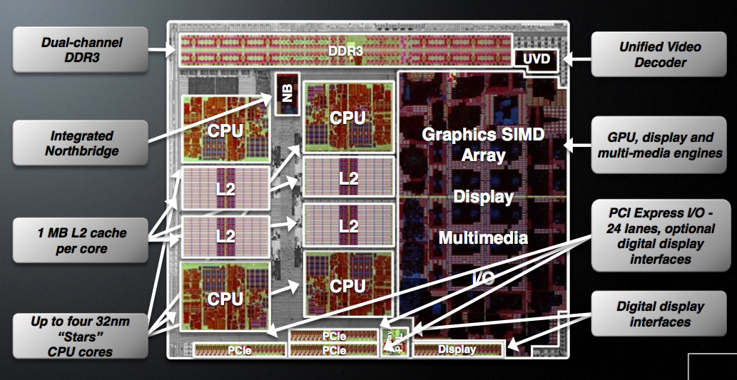
AMD is building two distinct versions of Llano, although only one will be available at launch. There's the quad-core, or big Llano, with four 32nm CPU cores and a 400 core GPU. This chip weighs in at 1.45 billion transistors, nearly 50% more than Sandy Bridge. Around half of the chip is dedicated to the GPU however, so those are tightly packed transistors resulting in a die size that's only 5% larger than Sandy Bridge.
| CPU Specification Comparison | ||||||||
| CPU | Manufacturing Process | Cores | Transistor Count | Die Size | ||||
| AMD Llano 4C | 32nm | 4 | 1.45B | 228mm2 | ||||
| AMD Llano 2C | 32nm | 2 | 758M | ? | ||||
| AMD Thuban 6C | 45nm | 6 | 904M | 346mm2 | ||||
| AMD Deneb 4C | 45nm | 4 | 758M | 258mm2 | ||||
| Intel Gulftown 6C | 32nm | 6 | 1.17B | 240mm2 | ||||
| Intel Nehalem/Bloomfield 4C | 45nm | 4 | 731M | 263mm2 | ||||
| Intel Sandy Bridge 4C | 32nm | 4 | 995M | 216mm2 | ||||
| Intel Lynnfield 4C | 45nm | 4 | 774M | 296mm2 | ||||
| Intel Clarkdale 2C | 32nm | 2 | 384M | 81mm2 | ||||
| Intel Sandy Bridge 2C (GT1) | 32nm | 2 | 504M | 131mm2 | ||||
| Intel Sandy Bridge 2C (GT2) | 32nm | 2 | 624M | 149mm2 | ||||
Given the transistor count, big Llano has a deceptively small amount of cache for the CPU cores. There is no large catch-all L3 and definitely no shared SRAM between the CPU and GPU, just a 1MB private L2 cache per core. That's more L2 cache than either the 45nm quad-core Athlon II or Phenom II parts.
Intel's Sandy Bridge die is only ~20% GPU
The little Llano is a 758 million transistor dual-core version with only 240 GPU cores. Cache sizes are unchanged; little Llano is just a smaller version for lower price points. Initially both quad- and dual-core parts will be serviced by the same 1.45B transistor die. Defective chips will have unused cores fused off and will be sold as dual-core parts. This isn't anything unusual, AMD, Intel and NVIDIA all use die harvesting as part of their overall silicon strategy. The key here is that in the coming months AMD will eventually introduce a dedicated little Llano die to avoid wasting fully functional big Llano parts on the dual-core market. This distinction is important as it indicates that AMD isn't relying on die harvesting in the long run but rather has a targeted strategy for separate market segments.
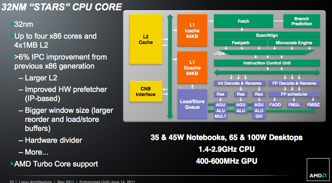
Architecturally AMD has made some minor updates to each Llano core. AMD is promising more than a 6% increase in instructions executed per clock (IPC) for the Llano cores vs. their 45nm Athlon II/Phenom II predecessors. The increase in IPC is due to the larger L2 cache, larger reorder and load/store buffers, new divide hardware, and improved hardware prefetchers.
On average I measured around a 3% performance improvement at the same clock speed as AMD's 45nm parts. Peak performance improved up to 14% however most of the gains were down in the 3—5% range. This is arguably the biggest problem that faces Llano. AMD's Phenom architecture debuted in 2007 and was updated in 2009. Llanos cores have been sitting around for the past 3-4 years with only a mild update while Intel has been through two tocks in the same timeframe. A ~6% increase in IPC isn't anywhere near close enough to bridge the gap left by Nehalem and Sandy Bridge.
Note that this comparison is without AMD's Turbo Core enabled, but more on that later.


177 Comments
View All Comments
duploxxx - Sunday, June 19, 2011 - link
talking about crap??? men you are good at that, as if you need a 2600K for some compiling and add a 6990 to an e-350.men you do know someting about computers :) your a joke
BushLin - Wednesday, June 22, 2011 - link
If you're going to accuse someone of talking crap (correctly or otherwise) it helps if you know the difference between you're and your when attempting to insult them.Broheim - Monday, June 27, 2011 - link
I use a fast CPU for compiling because I actually like being productive rather than just staring at the screen.my point about the 6990 was that a faster GPU != a better user experience for the vast majority of users, but logic seems to be lost on you.
Regenweald - Tuesday, June 14, 2011 - link
I'm currently playing the Witcher extended with a 2Ghz X2 ,a 4670 and 800 Mhz memory on a desktop with no complaints. In game settings medium and high. Are you saying that 2 more tweaked 32nm cores, 80 more shaders and ddr3 1600 or 1800 memory will not offer a good mobile gaming experience ? please.jollyjugg - Wednesday, June 15, 2011 - link
What kind of super computing application are you going to do in your laptop that you would need that "tremendous CPU power" that you are talking about. As somebody who has used both intel and amd machines for years I can tell you that for most user applications, you will hardly notice any difference in performance. The main complaint was that AMD machines were running hot particularly after intel cameup with power gating in nehalem in 2008. With this part you get a machine that runs way way cooler and almost 150- 200 bucks cheaper than comparable intel machines plus you get discrete quality graphics for free. Nobody can change cynics like you. Because you cant expect Intel to sell anything cheap you would want to AMD to sell things cheaper. Well if you want good things in life you should be prepared to pay. Dont write trash. Like gaming is not important for average user, tremendous computing power and 3 GHz CPU speed is also not important for the average PC user. But multimedia and movie rendering etc is. So go Llano!!!Seikent - Tuesday, June 14, 2011 - link
This platform offer some good things, but if the prices aren't low it won't go well. Now it's quite easy to find a sandy bridge notebook with discrete gpu for a few more dollars.If ACF does achieve to work like CF in the future, it would be great!
SteelCity1981 - Tuesday, June 14, 2011 - link
Finally we have an intergrated graphics solution that's worth really talking about.aegisofrime - Tuesday, June 14, 2011 - link
Judging by the performance, this part won't be priced very high. And that's a worry, considering that it packs 1.45 billion transistors. In comparison, Sandy Bridge is 995 million transistors, and sells for more money. Profit margins are gonna be tight on this one.JarredWalton - Tuesday, June 14, 2011 - link
AMD has a slide that points out that compared to their previous generation, they're packing a 66 mm2 Northbridge, 200 mm2 CPU, and 1080 mm2 dGPU into a 228 mm2 package. They've made money this past quarter, so this should do better than Athlon/Phenom II.JarredWalton - Tuesday, June 14, 2011 - link
Note: that's supposed to be 108 mm2 GPU, not 1080. Whoops.