The AMD Llano Notebook Review: Competing in the Mobile Market
by Jarred Walton & Anand Lal Shimpi on June 14, 2011 12:01 AM ESTThe Llano A-Series APU
Although Llano is targeted solely at the mainstream, it is home to a number of firsts for AMD. This is AMD's first chip built on a 32nm SOI process at GlobalFoundries, it is AMD's first microprocessor to feature more than a billion transistors, and as you'll soon see it's the first platform with integrated graphics that's actually worth a damn.
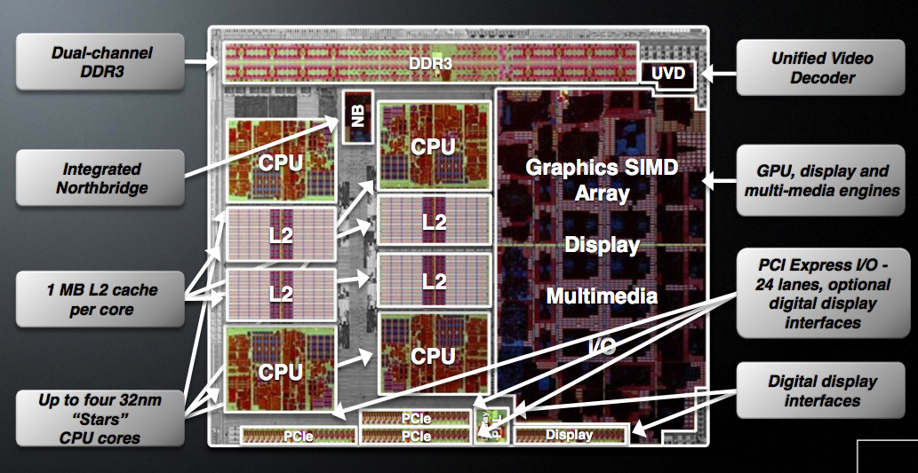
AMD is building two distinct versions of Llano, although only one will be available at launch. There's the quad-core, or big Llano, with four 32nm CPU cores and a 400 core GPU. This chip weighs in at 1.45 billion transistors, nearly 50% more than Sandy Bridge. Around half of the chip is dedicated to the GPU however, so those are tightly packed transistors resulting in a die size that's only 5% larger than Sandy Bridge.
| CPU Specification Comparison | ||||||||
| CPU | Manufacturing Process | Cores | Transistor Count | Die Size | ||||
| AMD Llano 4C | 32nm | 4 | 1.45B | 228mm2 | ||||
| AMD Llano 2C | 32nm | 2 | 758M | ? | ||||
| AMD Thuban 6C | 45nm | 6 | 904M | 346mm2 | ||||
| AMD Deneb 4C | 45nm | 4 | 758M | 258mm2 | ||||
| Intel Gulftown 6C | 32nm | 6 | 1.17B | 240mm2 | ||||
| Intel Nehalem/Bloomfield 4C | 45nm | 4 | 731M | 263mm2 | ||||
| Intel Sandy Bridge 4C | 32nm | 4 | 995M | 216mm2 | ||||
| Intel Lynnfield 4C | 45nm | 4 | 774M | 296mm2 | ||||
| Intel Clarkdale 2C | 32nm | 2 | 384M | 81mm2 | ||||
| Intel Sandy Bridge 2C (GT1) | 32nm | 2 | 504M | 131mm2 | ||||
| Intel Sandy Bridge 2C (GT2) | 32nm | 2 | 624M | 149mm2 | ||||
Given the transistor count, big Llano has a deceptively small amount of cache for the CPU cores. There is no large catch-all L3 and definitely no shared SRAM between the CPU and GPU, just a 1MB private L2 cache per core. That's more L2 cache than either the 45nm quad-core Athlon II or Phenom II parts.
Intel's Sandy Bridge die is only ~20% GPU
The little Llano is a 758 million transistor dual-core version with only 240 GPU cores. Cache sizes are unchanged; little Llano is just a smaller version for lower price points. Initially both quad- and dual-core parts will be serviced by the same 1.45B transistor die. Defective chips will have unused cores fused off and will be sold as dual-core parts. This isn't anything unusual, AMD, Intel and NVIDIA all use die harvesting as part of their overall silicon strategy. The key here is that in the coming months AMD will eventually introduce a dedicated little Llano die to avoid wasting fully functional big Llano parts on the dual-core market. This distinction is important as it indicates that AMD isn't relying on die harvesting in the long run but rather has a targeted strategy for separate market segments.
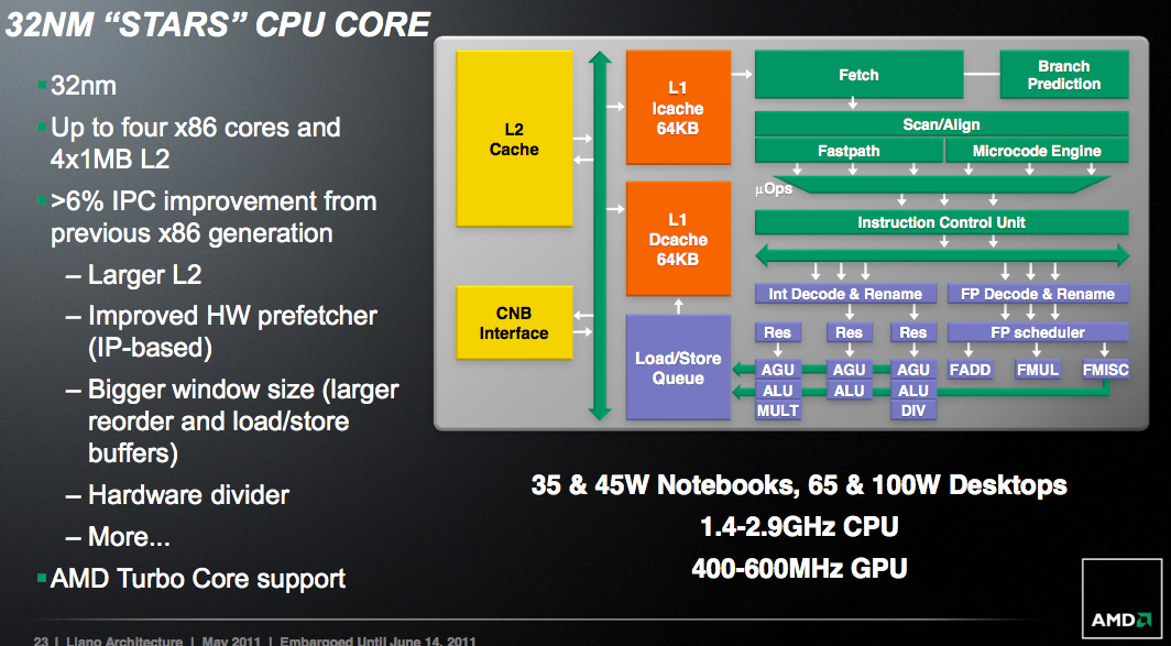
Architecturally AMD has made some minor updates to each Llano core. AMD is promising more than a 6% increase in instructions executed per clock (IPC) for the Llano cores vs. their 45nm Athlon II/Phenom II predecessors. The increase in IPC is due to the larger L2 cache, larger reorder and load/store buffers, new divide hardware, and improved hardware prefetchers.
On average I measured around a 3% performance improvement at the same clock speed as AMD's 45nm parts. Peak performance improved up to 14% however most of the gains were down in the 3—5% range. This is arguably the biggest problem that faces Llano. AMD's Phenom architecture debuted in 2007 and was updated in 2009. Llanos cores have been sitting around for the past 3-4 years with only a mild update while Intel has been through two tocks in the same timeframe. A ~6% increase in IPC isn't anywhere near close enough to bridge the gap left by Nehalem and Sandy Bridge.
Note that this comparison is without AMD's Turbo Core enabled, but more on that later.


177 Comments
View All Comments
Brian23 - Tuesday, June 14, 2011 - link
Jarred/Anand,Based on the benchmarks you've posted, It's not very clear to me how this CPU performs in "real world" CPU usage. Perhaps you have it covered with one of your synthetic benchmarks, but by looking at the names, it's not clear which ones stress the integer vs floating point portions of the processor.
IMO, a test I'd REALLY like to see is how this APU compares in a compile benchmark against a C2D 8400 and a i3 380M. Those are both common CPUs that can be used to compare against other benchmarks.
Could you compile something like Chrome or Firefox on this system and a couple others and update the review?
Thanks! I appreciate the work you guys do!
ET - Tuesday, June 14, 2011 - link
PCMark tests common applications. You can read more details here: http://www.pcmark.com/wp-content/uploads/2011/05/P...While I would find a compilation benchmark interesting, are you suggesting that this will be more "real world"? How many people would do that compared to browsing, video, gaming? Probably not a lot.
Brian23 - Tuesday, June 14, 2011 - link
Thanks for the link. I was looking for something that described what the synthetic benchmarks mean.As for "real world," it really depends from one user to the next. What I was really trying to say is that no-one buys a PC just to run benchmarks. Obviously the benchmark companies try to make their benchmarks simulate real world scenarios, but there's no way they can truly simulate a given person's exact workload because it's going to be different from someone else's workload.
If we're going down the synthetic benchmark path, what I'd like to see is a set of benchmarks that specifically stresses one aspect of a system. (i.e. integer unit or FPU.) That way you can compare processor differences directly without worrying about how other aspects of the system affect what you're looking at. In the case of this review, I was looking at the Computation benchmark listed. After reading the whitepaper, I found out that benchmark is stressing both the CPU and the GPU, so it's not really telling me just about the CPU which is the part I'm interested in.
Switching gears to actual real world tests, seeing a compile will tell me what I'm interested in: CPU performance. Like you said, most people aren't going to be doing this, but it's interesting because it will truly test just the CPU.
JarredWalton - Tuesday, June 14, 2011 - link
Hi Brian,I haven't looked into compiling code in a while, but can you give me a quick link to a recommended (free) Windows compiler for Chrome? I can then run that on all the laptops and add it to my benchmark list. I would venture to say that an SSD will prove more important than the CPU on compiling, though.
Brian23 - Tuesday, June 14, 2011 - link
Jarred,This link is a user's quick how-to for compiling chrome:
http://cotsog.wordpress.com/2009/11/08/how-to-comp...
This is the official chrome build instructions:
http://dev.chromium.org/developers/how-tos/build-i...
Both use Visual Studio Express which is free.
I really appreciate this extra work. :-)
krumme - Tuesday, June 14, 2011 - link
The first links at the top is sponsored3 times exactly the same i7 + 460 ! ROFL
Then 1 i7 with a 540
Damn - looks funny, but at least it not 1024 *768 like the preview, but the most relevant resolution for the market - thank you for that
Shadowmaster625 - Tuesday, June 14, 2011 - link
Man what is it with this dumb yuppie nonsense. No I dont want to save $200 because I dont actually work for my money. Hell, if you're even reading this site then it is highly likely that the two places you want more performance from your notebook is games and internet battery life. All this preening about intel's crippled cpu being 50% faster dont mean jack because ... well its a crippled cpu. It cant play games yet it has a stupid igp. Why get all yuppity about such an obvious design failure, so much so that you'd be willing to sneeze at a $200 savings like it means nothing. It actually means something to people who work for a living. Most people just dont need the extra 50% cpu speed from a notebook. But having a game that runs actually does mean something tangible.madseven7 - Tuesday, June 14, 2011 - link
I'm not sure why people think this is such a crappy cpu. Am I missing something? Wasn't the Llano APU that was tested the lowest of the A8 series with DDR 1333? Doesn't it give up 500MHz-800MHz to the SB notebooks that were tested? Wouldn't the A8 3530mx perform much better? I for one would love to see a review of the A8 3530mx personally.ET - Tuesday, June 14, 2011 - link
Good comment. This is the highest end 35W CPU, but not the highest end Llano. So it gets commended for battery life but not performance. It will be interesting to see the A8-3530MX results for performance and battery life. It would still lose to Sandy Bridge quite soundly on many tests, I'm sure, but it's still a significant difference in clock speed over the A8-3500M..Jasker - Tuesday, June 14, 2011 - link
One thing that is really interesting that isn't brought up here is the amount of power used during gaming. Not only do you get much better gaming than Intel, but you also get much less power. Double whammy.