Intel’s 2011 Investor Meeting - Intel’s Architecture Group: 14nm Airmont Atom In 2014
by Ryan Smith on May 17, 2011 6:27 PM ESTToday Intel is holding their annual investors meeting at their Santa Clara headquarters. In true Intel fashion it’s being treated as a big event (ed: it’s so big they ran out of lunch), as this is the company’s primary vehicle for addressing the investors holding their 125 billion dollars in shares; in essence it’s a reprise of their current and future technology plans as a pep-talk for investors. As such it’s not really a technical event, but it’s not uncommon for a few new technical details to shake out during the presentations.
There are a number of presentations throughout the day, including keynotes from Paul Otellini, and presentations from a number of Intel groups including the architecture group, the data center group, and the manufacturing group. If something is going to shake out it’s bound to be the architecture group, so this is where we’ll start.
Atom/SoC
A big part of the architecture group’s discussion focused on Atom/SoC. The 32nm Medfield Atom is due this year, so Intel has been laying out their plans for what they’re going to be doing with Medfield. Unsurprisingly, a big push with Medfield is to break into the SoC space in a way that Moorestown could not. Intel never managed any major design wins for smartphones with Moorestown, which is something they want to correct with Medfield. To that extent Intel has been showing off Medfield concept phones to show investors that it’s a viable product and to try to drum up support.

Intel's Medfield Concept Phone
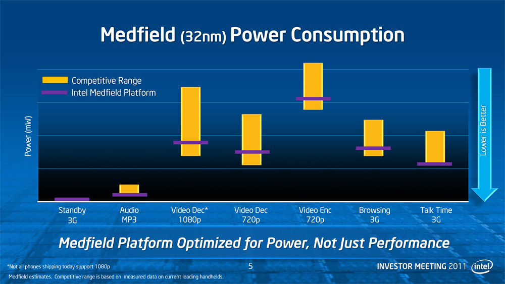
Intel is also spending some effort to dispel the idea that they can’t be competitive on a power consumption basis; in fact for the amount of effort they put into that message and the number of times they repeated it, they seem to be seriously concerned about being perceived as uncompetitive. Intel did some power consumption testing on Medfield and put together a slide showing their findings that Medfield is competitive with some current leading phones, but as always take this with a pinch of salt. Ultimately this is a comparison of 32nm Medfield with 4Xnm ARM SoCs, so it’s only applicable so long as Intel’s still ahead of the ARM producers on manufacturing technology.
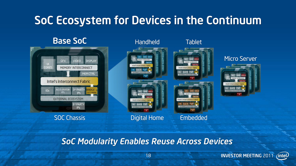
Moving on, one thing Intel has been dealing with as Atom has evolved is how to consolidate all the disparate parts of a system onto a SoC, given the wide variety of uses for a SoC. With discrete components manufacturers could simply build a device out of the parts necessary for the features they need, but with Atom SoCs much of that gets shifted onto Intel. For Intel this means they will be focusing on producing a wider variety of SoCs, based on building up individual SoC designs on a modular basis. Intel isn’t going in-depth on how many specific SoC variants they’re planning on offering, but our impression is that there will be many variants, similar to how Intel offers a number of different desktop/laptop/server CPUs based on a common architecture.
Finally, Intel published a new generalized roadmap for Atom through 2014. Unfortunately they aren’t going into any significant detail on architecture here – while Silvermont is named, nothing is confirmed besides the name and manufacturing process – but it’s a start, and it ends with a shocker. We will see Silvermont in 2013 on Intel’s 22nm process, likely hand-in-hand with Intel’s aforementioned plans for additional SoC variations.
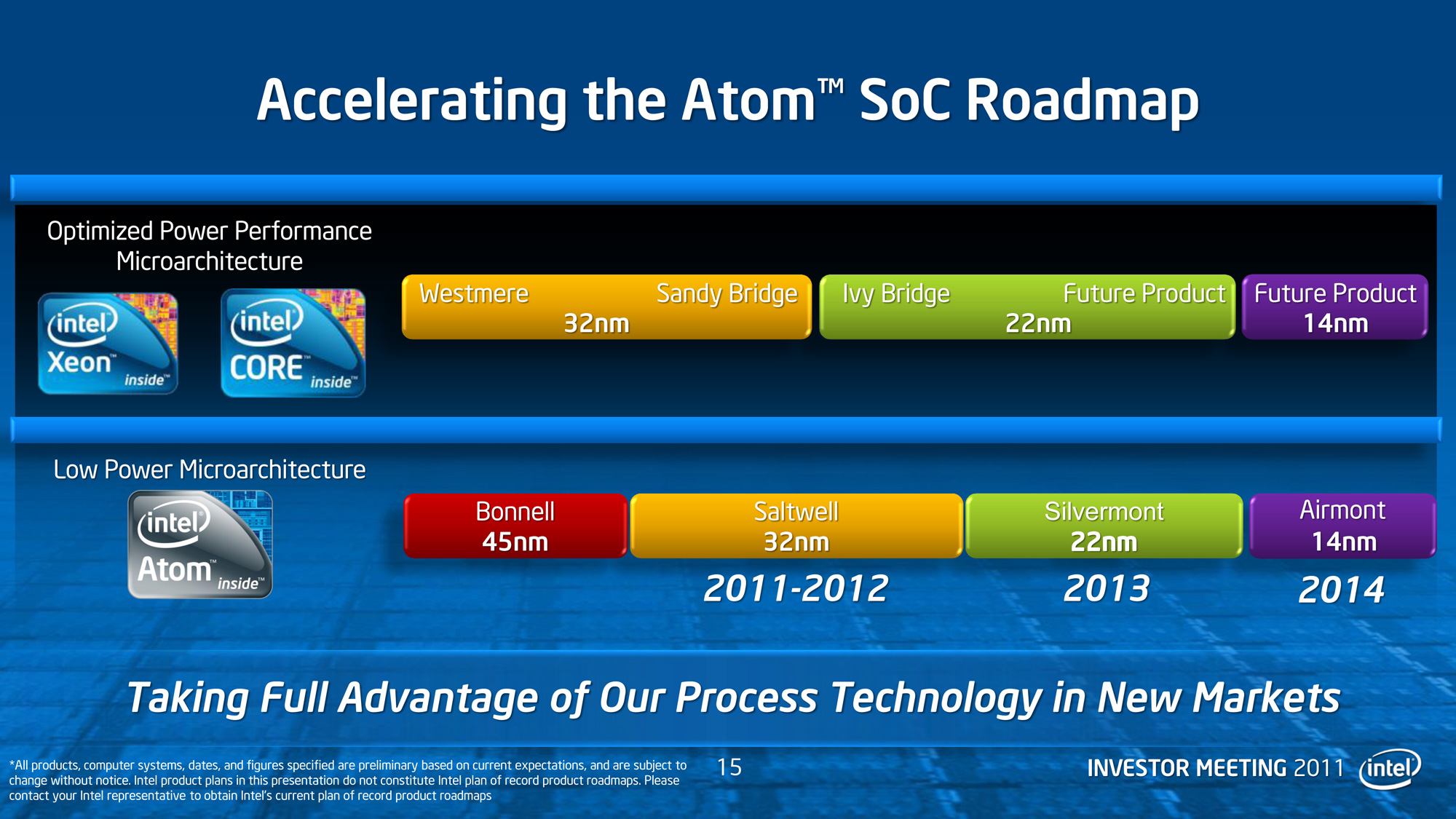
Far more interesting however is that Intel didn’t stop with Silvermont on their Atom roadmap. Intel’s roadmap goes out to 2014 and includes Silvermont’s successor: Airmont. We know even less about Airmont than we do Silvermont, but a good guess would be that it’s the tick in Intel’s tick-tock cadence for Atom. The biggest news here is that with a move to tick-tock for Atom, Intel is finally accelerating the production of Atom parts on their newer fab processes. Currently Atom processors are a year or more behind Core processors for using a new process, and even with Silvermont that’s still going to be the case. But for Airmont that window is shrinking: Airmont will be released on Intel’s forthcoming 14nm process in 2014, the same year as their respective Core processor. Intel hasn’t specified when in 2014 this will be, and it’s likely it will still be months after 14nm launches for Core processors, but nevertheless it’s much sooner than it has been before.
By accelerating their production of Atom on new processes, this should allow Intel to capitalize on their manufacturing advantages over the rest of the fabs. With Intel’s existing Atom schedule, they only have a year or less before other fabs catch up with them, so by putting Atoms on new processes sooner, they increase that lead time. So far Intel’s ARM SoC competitors have really only had to deal with Intel’s threats on an architectural level, so having Intel challenge them at a manufacturing level too will make Intel a much more threatening competitor.
Core
Meanwhile, for the rest architecture group’s presentation, it was largely a catch-all for all of Intel’s consumer technologies. Much of the talk focused on where Intel plans to be in the next few years, based on where they expect to be thanks to their newly announced 22nm process. Intel considers their 22nm process to be a significant advantage for their products, so a great deal of their plans in the consumer space involve exploiting it in some manner or another.
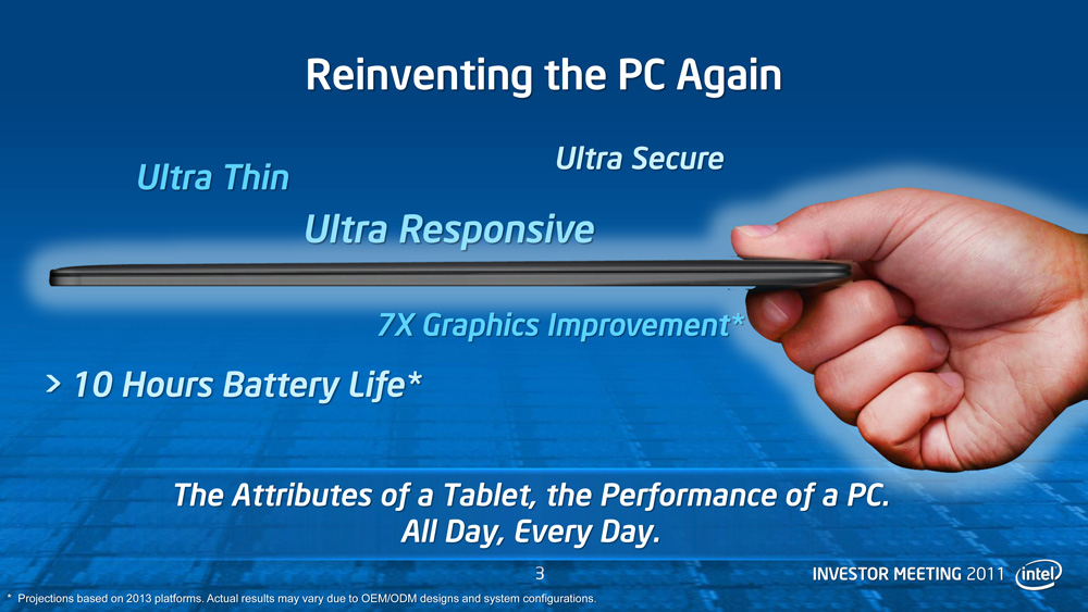
Ivy Bridge, Intel’s first 22nm product, is being shown off in a few sample systems with Intel reiterating that it will be launching at the beginning of next year – we’d guess at CES. Longer term, Intel wants to get laptops closer to netbooks/tablets in terms of size and battery life, so that they can push 10 hours on a laptop (something the C2D-based Macbook Air can already get very close to). The catalyst for this will be Haswell, Intel’s new microarchitecture on their 22nm process scheduled for 2013.
Intel also used the occasion to show off a couple new technologies that they’re working on for Ivy Bridge generation computers. We’ve heard the name Fast Flash Standby mentioned before, but as far as we know this was the first time it has been demoed. In a nutshell, Fast Flash Standby is hibernating to SSDs, another product Intel has a significant interest in. The basis for Fast Flash Standby is that while going into sleep is fast, it requires leaving the RAM powered up to hold its contents, which is why sleep is only good for a few days of standby versus weeks for hibernation. Hibernating to a SSD, particularly one with a very high sequential read and write throughput, allows hibernation to take place much quicker and to resume much sooner. Intel is doing more here than just writing a hibernation file to a SSD, but the concept is similar.
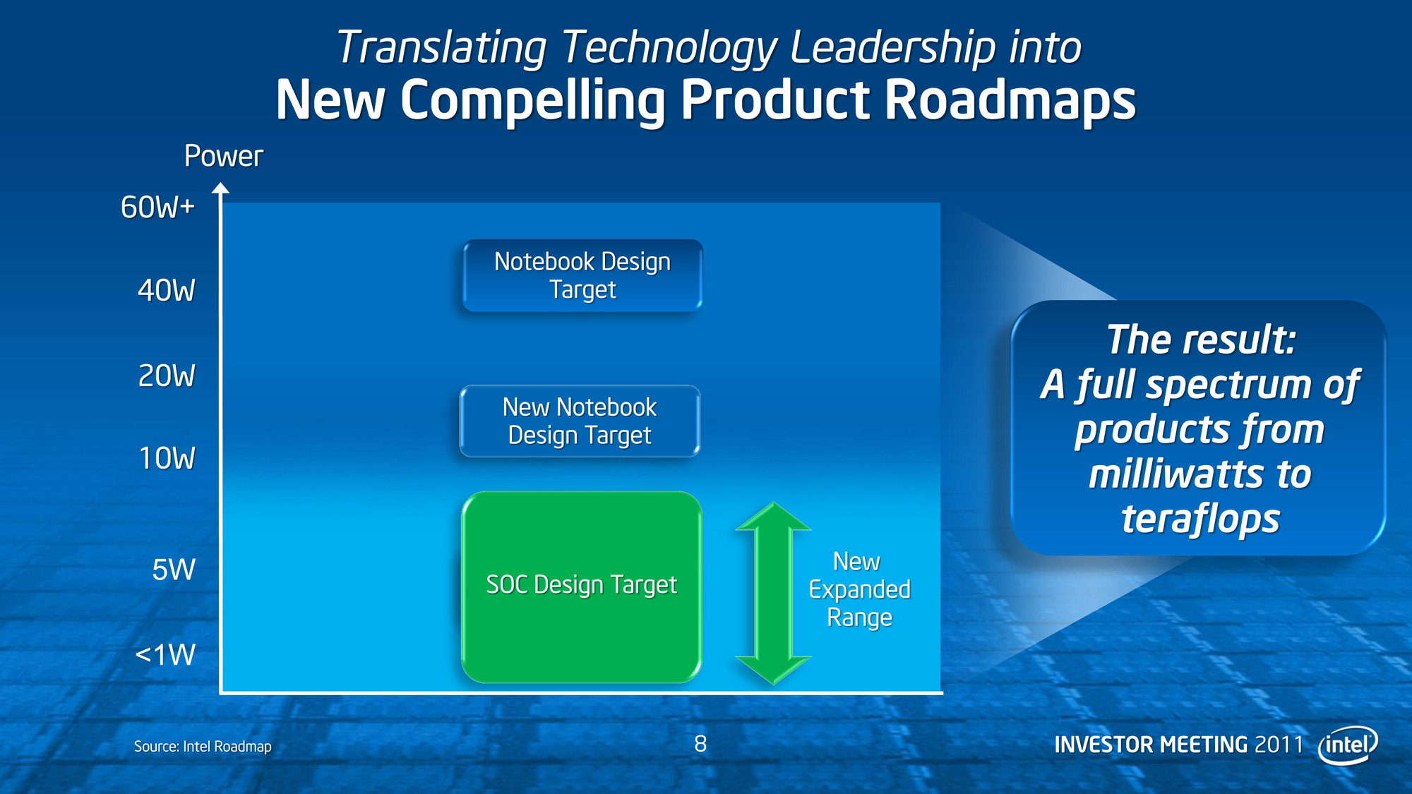
Longer term Intel is looking at what kind of markets they want to go after, and what architectures they need to reach them. Intel is talking – albeit nebulously – about a new 10-20W notebook design target to sit right above their sub-10W target for Atom/SoC. Currently Intel offers CULV Sandy Bridge processors in the 10-20W range, but Intel appears to want to go beyond CULV with this new target. Whether this is a bulked up Atom, or a further trimmed IB/Haswell/Skylake remains to be seen. Intel is throwing around some performance targets however: they’re looking to improve iGPU performance by 12x over today’s performance in that 10-20W envelope.


63 Comments
View All Comments
SteelCity1981 - Wednesday, May 18, 2011 - link
Intel has been blind sided by ARM. I guess Intels cocky attitude has got the better of them and now all of a sudden they are feeling the heat from ARM and even AMD in the Micro device sector.Stuka87 - Wednesday, May 18, 2011 - link
Well Intel sat around for years with basically no changes to the Atom. Yes they added a dual core model, and hyper threading, but neither of those are architectural changes.This gave ARM and AMD time to develop their own products to compete in the same market. They now have a head start and Intel has to play catch up. But with as much money as Intel has, I doubt it will take them long to catch back up.
DanNeely - Wednesday, May 18, 2011 - link
Intel needed process shrinks to get the atom's die size small enough to play in the smart phone arena. Architecture changes that would make it larger again would have been counter productive.For comparison the Tegra 2 (only dual core a9 I could find numbers on) is 260M, with the cpus only taking 10% of the total. The original single core atoms were 47M transistors for what was basically just the CPU, D510 atom is 176m transistors and presumably uses roughly half its transistors on the CPU cores. I couldn't find a transistor count for the NM10 southbridge, but assuming the transistor count is proportional to the package size (weak assumption but I don't have anything better) it would have about 115M transistors. Granted not all of them are for things needed in a smartphone/tablet OTOH it also lacks some things one would need; but at 45nm the atom platform barely has transistor parity and has significantly less transistors to use for things like the GPU.
It won't be until the 32nm shrink that Intel will be able to get enough transistors to catch up on the GPU size. Coming from the other direction, the Cortex A15 is a much more complex design and will presumably be significantly larger, reducing Intels dependence on the process advantage/raw CPU power to be competitive.
L. - Thursday, May 19, 2011 - link
Well you're wrong to doubt.How long has Intel tried to make gfx ?
How far are they ?
Quite a while and nowhere are the answers ...
And there are quite a few markets Intel is not going to win anytime soon, and I suspect they will lose the SSD market within the next five years aswell, they're behind on controller tech and they're clearly not the only ones with high quality NAND fabs.
The reason Intel would remain on top would be that we know they can redo what they did in the Athlon era: playing dirty, and doing it damn well.
That Intel was able to pass through an era of more than 3 years of technological inferiority without suffering any heavy market losses is the proof they are financially solid - that doesn't help with the tech though, even if the core era has been quite strong since.
JasonInofuentes - Sunday, May 22, 2011 - link
While their graphics efforts (more on this and a few other things later) haven't yielded a supremely viable product they have improved an awful lot while lowering their power envelope. Further, they are willing, and this is something they should get a lot of respect for, to put their research to good use no matter what it's original intent. Larrabee was introduced as their move towards high end graphics, and while it was canceled as a stand alone product it is still a big focus in their efforts to compete in HPC. As we know now, Conroe was the result of an exercise in developing mobile chips, a move they made well ahead of the markets move towards laptops as the workhorses of our tech ecology.Think of it this way, Intel squeezes something out of every bit of research they do, so even if their SoC's don't compete with ARM, they will use the technology to move the goal line forward somewhere.
j108b - Wednesday, May 18, 2011 - link
Now I just hope that Intel will give real confirmation if Ivy Bridge (s1155) will work on existing chipsets.L. - Thursday, May 19, 2011 - link
Intel + long-term platform = boom.dragosmp - Wednesday, May 18, 2011 - link
About:"The basis for Fast Flash Standby is that while going into sleep is fast, it requires leaving the RAM powered up to hold its contents, which is why sleep is only good for a few days of standby versus weeks for hibernation."
I agree with your assessment about "Sleep", but to you say "Hibernation" holds for a few weeks is wrong. Hibernation = Shut Down from the battery life perspective; a computer can stay in Hibernation mode indefinitely and it would not consume any more battery than if it were Shut down. One can dismantle a rig, rebuild it and the rig will resume from Hibernation. I have done with mine a few years ago: dismantled, packed, flown by plane, rebuilt and it resumed exactly where it left off.
I am writing this post as some users seem to think Hibernation is some sort of deeper-Sleep and quantifying the battery life under Hibernation vs in Sleep mode only supports this misconception. Intel's tech is of doubtful usage as now if a computer has an SSD as OS drive and Hibernation mode enabled then this Fast Flash Standby already exists.
Ryan Smith - Wednesday, May 18, 2011 - link
I don't disagree with you (Jarred could say more, this is his specialty). However those numbers specifically came from Intel.L. - Thursday, May 19, 2011 - link
Quite simply Ryan, hibernation is this :-> Write all RAM contents to hiberfil.sys
-> Force Shutdown
Then when you go out of it :
-> Load OS
-> Load back all RAM
And there you go.
Because of that, you can hibernate as long as your storage device (hdd or ssd or anything you'd like to use) can live, quite a lot yes.
Intel can say any random shit they want, they did not write the windows hibernation thingy, so the only real info you can get is @ microsoft.