Intel’s 2011 Investor Meeting - Intel’s Architecture Group: 14nm Airmont Atom In 2014
by Ryan Smith on May 17, 2011 6:27 PM ESTToday Intel is holding their annual investors meeting at their Santa Clara headquarters. In true Intel fashion it’s being treated as a big event (ed: it’s so big they ran out of lunch), as this is the company’s primary vehicle for addressing the investors holding their 125 billion dollars in shares; in essence it’s a reprise of their current and future technology plans as a pep-talk for investors. As such it’s not really a technical event, but it’s not uncommon for a few new technical details to shake out during the presentations.
There are a number of presentations throughout the day, including keynotes from Paul Otellini, and presentations from a number of Intel groups including the architecture group, the data center group, and the manufacturing group. If something is going to shake out it’s bound to be the architecture group, so this is where we’ll start.
Atom/SoC
A big part of the architecture group’s discussion focused on Atom/SoC. The 32nm Medfield Atom is due this year, so Intel has been laying out their plans for what they’re going to be doing with Medfield. Unsurprisingly, a big push with Medfield is to break into the SoC space in a way that Moorestown could not. Intel never managed any major design wins for smartphones with Moorestown, which is something they want to correct with Medfield. To that extent Intel has been showing off Medfield concept phones to show investors that it’s a viable product and to try to drum up support.

Intel's Medfield Concept Phone
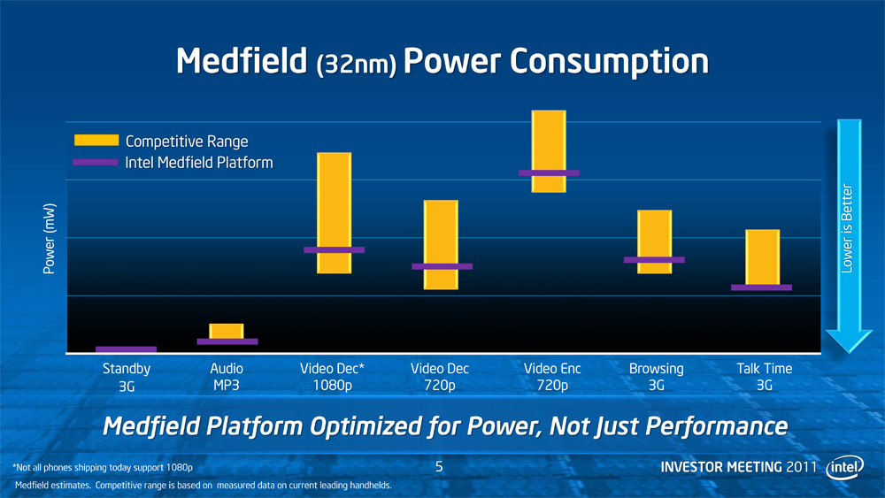
Intel is also spending some effort to dispel the idea that they can’t be competitive on a power consumption basis; in fact for the amount of effort they put into that message and the number of times they repeated it, they seem to be seriously concerned about being perceived as uncompetitive. Intel did some power consumption testing on Medfield and put together a slide showing their findings that Medfield is competitive with some current leading phones, but as always take this with a pinch of salt. Ultimately this is a comparison of 32nm Medfield with 4Xnm ARM SoCs, so it’s only applicable so long as Intel’s still ahead of the ARM producers on manufacturing technology.
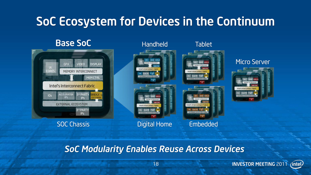
Moving on, one thing Intel has been dealing with as Atom has evolved is how to consolidate all the disparate parts of a system onto a SoC, given the wide variety of uses for a SoC. With discrete components manufacturers could simply build a device out of the parts necessary for the features they need, but with Atom SoCs much of that gets shifted onto Intel. For Intel this means they will be focusing on producing a wider variety of SoCs, based on building up individual SoC designs on a modular basis. Intel isn’t going in-depth on how many specific SoC variants they’re planning on offering, but our impression is that there will be many variants, similar to how Intel offers a number of different desktop/laptop/server CPUs based on a common architecture.
Finally, Intel published a new generalized roadmap for Atom through 2014. Unfortunately they aren’t going into any significant detail on architecture here – while Silvermont is named, nothing is confirmed besides the name and manufacturing process – but it’s a start, and it ends with a shocker. We will see Silvermont in 2013 on Intel’s 22nm process, likely hand-in-hand with Intel’s aforementioned plans for additional SoC variations.
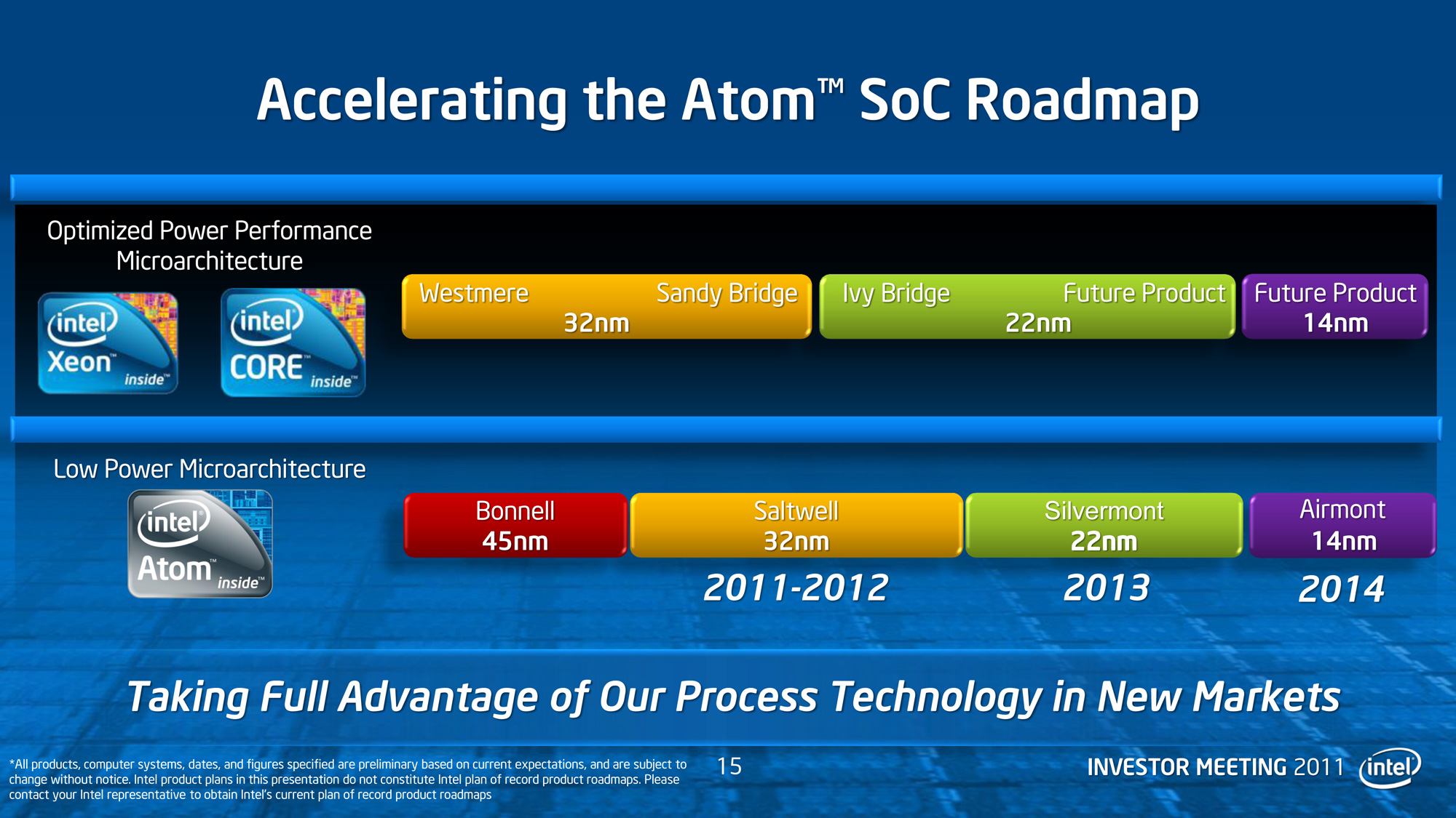
Far more interesting however is that Intel didn’t stop with Silvermont on their Atom roadmap. Intel’s roadmap goes out to 2014 and includes Silvermont’s successor: Airmont. We know even less about Airmont than we do Silvermont, but a good guess would be that it’s the tick in Intel’s tick-tock cadence for Atom. The biggest news here is that with a move to tick-tock for Atom, Intel is finally accelerating the production of Atom parts on their newer fab processes. Currently Atom processors are a year or more behind Core processors for using a new process, and even with Silvermont that’s still going to be the case. But for Airmont that window is shrinking: Airmont will be released on Intel’s forthcoming 14nm process in 2014, the same year as their respective Core processor. Intel hasn’t specified when in 2014 this will be, and it’s likely it will still be months after 14nm launches for Core processors, but nevertheless it’s much sooner than it has been before.
By accelerating their production of Atom on new processes, this should allow Intel to capitalize on their manufacturing advantages over the rest of the fabs. With Intel’s existing Atom schedule, they only have a year or less before other fabs catch up with them, so by putting Atoms on new processes sooner, they increase that lead time. So far Intel’s ARM SoC competitors have really only had to deal with Intel’s threats on an architectural level, so having Intel challenge them at a manufacturing level too will make Intel a much more threatening competitor.
Core
Meanwhile, for the rest architecture group’s presentation, it was largely a catch-all for all of Intel’s consumer technologies. Much of the talk focused on where Intel plans to be in the next few years, based on where they expect to be thanks to their newly announced 22nm process. Intel considers their 22nm process to be a significant advantage for their products, so a great deal of their plans in the consumer space involve exploiting it in some manner or another.
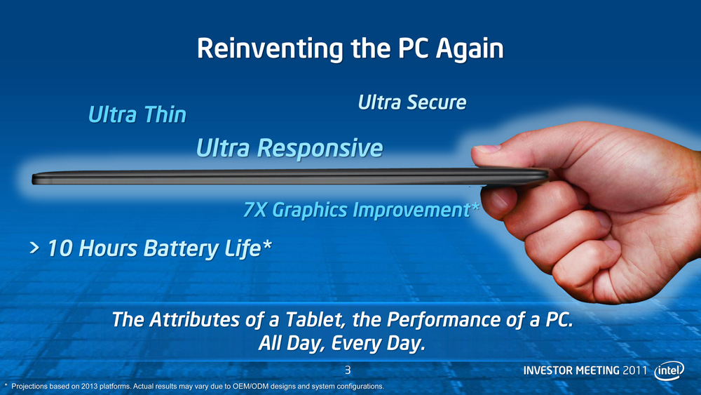
Ivy Bridge, Intel’s first 22nm product, is being shown off in a few sample systems with Intel reiterating that it will be launching at the beginning of next year – we’d guess at CES. Longer term, Intel wants to get laptops closer to netbooks/tablets in terms of size and battery life, so that they can push 10 hours on a laptop (something the C2D-based Macbook Air can already get very close to). The catalyst for this will be Haswell, Intel’s new microarchitecture on their 22nm process scheduled for 2013.
Intel also used the occasion to show off a couple new technologies that they’re working on for Ivy Bridge generation computers. We’ve heard the name Fast Flash Standby mentioned before, but as far as we know this was the first time it has been demoed. In a nutshell, Fast Flash Standby is hibernating to SSDs, another product Intel has a significant interest in. The basis for Fast Flash Standby is that while going into sleep is fast, it requires leaving the RAM powered up to hold its contents, which is why sleep is only good for a few days of standby versus weeks for hibernation. Hibernating to a SSD, particularly one with a very high sequential read and write throughput, allows hibernation to take place much quicker and to resume much sooner. Intel is doing more here than just writing a hibernation file to a SSD, but the concept is similar.
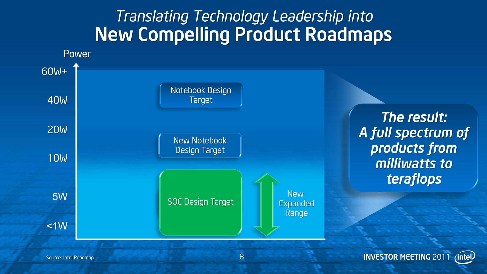
Longer term Intel is looking at what kind of markets they want to go after, and what architectures they need to reach them. Intel is talking – albeit nebulously – about a new 10-20W notebook design target to sit right above their sub-10W target for Atom/SoC. Currently Intel offers CULV Sandy Bridge processors in the 10-20W range, but Intel appears to want to go beyond CULV with this new target. Whether this is a bulked up Atom, or a further trimmed IB/Haswell/Skylake remains to be seen. Intel is throwing around some performance targets however: they’re looking to improve iGPU performance by 12x over today’s performance in that 10-20W envelope.


63 Comments
View All Comments
DanNeely - Wednesday, May 18, 2011 - link
The truth is far more prosaic. Like in all instruction sets that were originally designed on the CISC model, some x86 instructions require much more work than others do. To keep the CPU from running much more slowly than it needed to 99% of the time implementing the instructions in microcode and then using more RISC like execution units internally is the obvious way to go.Lest you think that means RISC "won" the architecture war, MMX, SSE, and more recently on die IGPs as specialized instruction sets for specific subsets of the work are a CISC concept. The war ended when die space grew large enough to combine the best of both worlds on a single chip.
wumpus - Friday, May 20, 2011 - link
The real driver of the CISC school of though was to make writing assembler as easy as a high level language (google "closing the semantic gap"). That idea is dead and buried. The only other issue that CISC might try to do is to reduce size of code. In modern terms, that means the pressure on the instruction cache (I could code hello world into a <20 byte .COM file in assembler. Don't ask what it compiles to now).SSE, MMX and all are a revival of vector design. The big catch is that CRAY machines included scatter/gather functions to access memory better. Not going to happen on current designs. The "latest thing" is the fused multiply-add (don't watch as intel and AMD botch the standard), which has been a DSP concept since forever. I suppose that all these ideas work to reduce the size of the inner loops (in bytes), but I wouldn't call them "CISC concepts, since often they appeared on RISC machines first.
ibudic1 - Wednesday, May 18, 2011 - link
about 2016...At the beginning of the 2015 it will be obvious that the production of oil will drop by about 3% / year. Google Peak Oil. Since energy is inelastic in terms of price, this will send the prices of everything through the roof, and the world economy will be close to or will collapse.
So if for no other technical reason I doubt that we will be seeing 10/11 nm soon or ever. If we do see 10/11 nm it will be many years down the road, probably not before 2020. A little after that or at about the same time US will have lost its dominance in both economic and military power as a world leader. - I've read an article from some CIA analyst claiming this.
So be ready for 2015+.
Thermogenic - Friday, May 20, 2011 - link
Well, if you read it on the Internet, I guess that means it has to be true!ibudic1 - Sunday, May 22, 2011 - link
Hm... where do you get your info?Your friend? Books? Newspapers? What's your point? Wiki articles for the uninitiated.
http://en.wikipedia.org/wiki/Quantum_tunnelling
http://en.wikipedia.org/wiki/Peak_oil
http://en.wikipedia.org/wiki/Supply_and_demand.
Thank you.
L. - Thursday, May 19, 2011 - link
The age of Moore's Law will extend far beyond the limits of the current litographic process family, as there are many other ways to go faster, many unexploited yet because they were not the (only) best choice.GullLars - Tuesday, May 24, 2011 - link
Moore's Law describes the transistor density at the most optimal cost/transistor point, not power or speed of said transistors. If you could find a way to double transistor density at the same cost every 18 months without shrinking the transistor size, it would still count.Solving some problems can be improved with near perfect scaling by more transistors, other problems quickly experience diminishing returns. This makes the case for the necessity of faster transistors. Many problems are not optimized in the way they are being solved today, and still has a lot of potential there. Moore's law alone is not the fate of the computational industry, although it has been the driver of a gloden age.
Jacmert - Wednesday, May 18, 2011 - link
- "Also is anyone else nervous about 3 gate transistors?"What I'm worried about is the 4 gate push. We'll probably see less of that now, though, since Blizzard nerfed the warp gate research time in the last patch. #starcraft2
Ammaross - Wednesday, May 18, 2011 - link
- "Also is anyone else nervous about 3 gate transistors?"More "gates" = more accurate signaling at higher speeds or lower voltages. The more accurate or low power a specific set of transistors need to be, the more gates they'll put (up to 5 was mentioned...). The usual is likely going to float in the 2-3 range.
L. - Thursday, May 19, 2011 - link
Good .. I'll go back to Queen rushing then ;)